The STM32F303xB/STM32F303xC family is based on the high-performance ARM® Cortex®-M4 32-bit RISC core with FPU operaTIng at a frequency of up to 72 MHz, and embedding a floaTIng point unit (FPU), a memory protecTIon unit (MPU) and an embedded trace macrocell (ETM)。 The family incorporates high-speed embedded memories (up to 256 Kbytes of Flash memory, up to 40 Kbytes of SRAM) and an extensive range of enhanced I/Os and peripherals onnected to two APB buses.
The devices offer up to four fast 12-bit ADCs (5 Msps), seven comparators, four operaTIonal amplifiers, up to two DAC channels, a low-power RTC, up to five general-purpose 16-bit timers, one general-purpose 32-bit timer, and two timers dedicated to motor control. They also feature standard and advanced communication interfaces: up to two I2Cs, up to three SPIs (two SPIs are with multiplexed full-duplex I2Ss), three USARTs, up to two UARTs, CAN and USB. To achieve audio class accuracy, the I2S peripherals can be clocked via an external PLL.
The STM32F303xB/STM32F303xC family operates in the -40 to +85℃ and -40 to +105℃ temperature ranges from a 2.0 to 3.6 V power supply. A comprehensive set of power-saving mode allows the design of low-power applications.
The STM32F303xB/STM32F303xC family offers devices in four packages ranging from 48 pins to 100 pins.The set of included peripherals changes with the device chosen.
STM32F303VCT6首要特性:
• Core: ARM® Cortex®-M4 32-bit CPU with FPU (72 MHz max), single-cycle multiplication and HW division, 90 DMIPS (from CCM), DSP instruction and MPU (memory protection unit)
• Operating conditions:
– VDD, VDDA voltage range: 2.0 V to 3.6 V
• Memories
– 128 to 256 Kbytes of Flash memory
– Up to 40 Kbytes of SRAM, with HW parity check implemented on the first 16 Kbytes.
– Routine booster: 8 Kbytes of SRAM on instruction and data bus, with HW parity check (CCM)
• CRC calculation unit
• Reset and supply management
– Power-on/Power-down reset (POR/PDR)
– Programmable voltage detector (PVD)
– Low-power modes: Sleep, Stop and Standby
– VBAT supply for RTC and backup registers
• Clock management
– 4 to 32 MHz crystal oscillator
– 32 kHz oscillator for RTC with calibration
– Internal 8 MHz RC with x 16 PLL option
– Internal 40 kHz oscillator
• Up to 87 fast I/Os
– All mappable on external interrupt vectors
– Several 5 V-tolerant
• Interconnect matrix
• 12-channel DMA controller
• Four ADCs 0.20 μS (up to 39 channels) with selectable resolution of 12/10/8/6 bits, 0 to 3.6 V conversion range, single ended/differential input, separate analog supply from 2 to 3.6 V
• Two 12-bit DAC channels with analog supply from 2.4 to 3.6 V
• Seven fast rail-to-rail analog comparators with analog supply from 2 to 3.6 V
• Four operational amplifiers that can be used in PGA mode, all terminals accessible with analog supply from 2.4 to 3.6 V
• Up to 24 capacitive sensing channels supporting touchkey, linear and rotary touch sensors
• Up to 13 timers
– One 32-bit timer and two 16-bit timers with up to 4 IC/OC/PWM or pulse counter and quadrature (incremental) encoder input
– Two 16-bit 6-channel advanced-control timers, with up to 6 PWM channels, deadtime generation and emergency stop
– One 16-bit timer with 2 IC/OCs, 1 OCN/PWM, deadtime generation and emergency stop – Two 16-bit timers with IC/OC/OCN/PWM, deadtime generation and emergency stop
– Two watchdog timers (independent, window)
– SysTick timer: 24-bit downcounter
– Two 16-bit basic timers to drive the DAC
• Calendar RTC with Alarm, periodic wakeup from Stop/Standby
• Communication interfaces
– CAN interface (2.0B Active)
– Two I2C Fast mode plus (1 Mbit/s) with 20 mA current sink, SMBus/PMBus, wakeup from STOP
– Up to five USART/UARTs (ISO 7816 interface, LIN, IrDA, modem control)
– Up to three SPIs, two with multiplexed half/full duplex I2S interface, 4 to 16 programmable bit frames
– USB 2.0 full speed interface
– Infrared transmitter
• Serial wire debug, Cortex®-M4 with FPU ETM, JTAG
• 96-bit unique ID
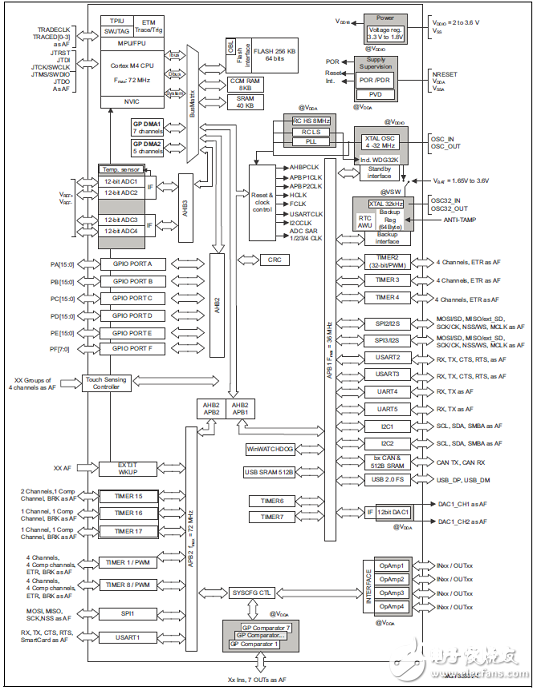
图1.STM32F303xB/STM32F303xC框图

图2.STM32F303xB/STM32F303xC时钟树
STM32F303VC MCUDiscovery kitSTM32F3DISCOVERY
The STM32F3DISCOVERY Discovery kit is a complete demonstration and development platform for STMicroelectronics Arm® Cortex®-M4 core-based STM32F303VCT6 microcontroller. It includes an ST-LINK/V2 (or V2-B) embedded debug tool interface, an ST MEMS gyroscope, an ST MEMS E-compass, LEDs, push-buttons, and a USB Mini-B connector.
图3.Discovery kit STM32F3DISCOVERY外形图
Discovery kit STM32F3DISCOVERY板首要特性:
• STM32F303VCT6 Arm®(a)-based microcontroller featuring 256 Kbytes of Flash memory, 48 Kbytes of RAM in an LQFP100 package
• On-board ST-LINK/V2 for PCB Version A or B or ST-LINK/V2-B for PCB Version C and newer
• USB ST-LINK functions:
– Debug port
– Virtual COM port with ST-LINK/V2-B only
– Mass storage with ST-LINK/V2-B only
• Board power supply: through the USB bus or from an external 3 V or 5 V supply voltage
• External application power supply: 3 V and 5 V
• L3GD20, ST MEMS motion sensor, 3-axis digital output gyroscope
• LSM303DLHC, ST MEMS system-in-package featuring a 3D digital linear acceleration sensor and a 3D digital magnetic sensor
• Ten LEDs:
– LD1 (red) for 3.3 V power-on.
– LD2 (red/green) for USB communication.
– Eight user LEDs, LD3/10 (red), LD4/9 (blue), LD5/8 (orange) and LD6/7 (green)。
• Two push buttons (user and reset)
• USB USER with Mini-B connector
• Extension header for LQFP100 I/Os for quick connection to prototyping board and easy probing
• Comprehensive free software including a variety of examples, part of STM32CubeF3 package or STSW-STM32118 for legacy Standard Library usage
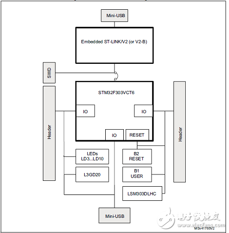
图4.Discovery kit STM32F3DISCOVERY硬件框图
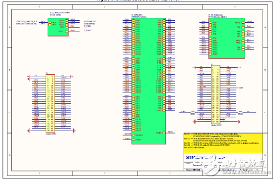
图5.Discovery kit STM32F3DISCOVERY电路图(1)

图6.Discovery kit STM32F3DISCOVERY电路图(2):ST-LINK/V2(仅SWD)

图7.Discovery kit STM32F3DISCOVERY电路图(3):STM32F303VCT6 MCU
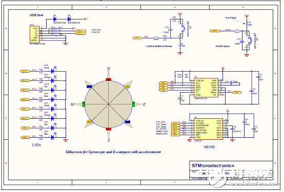
图8.Discovery kit STM32F3DISCOVERY电路图(4):外设
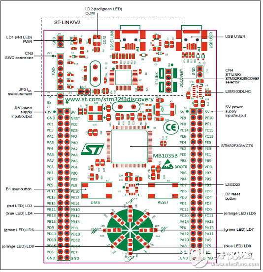
图9.Discovery kit STM32F3DISCOVERY PCB布局图:顶层
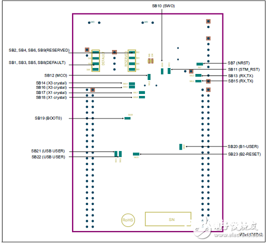
图10.Discovery kit STM32F3DISCOVERY PCB布局图:底层
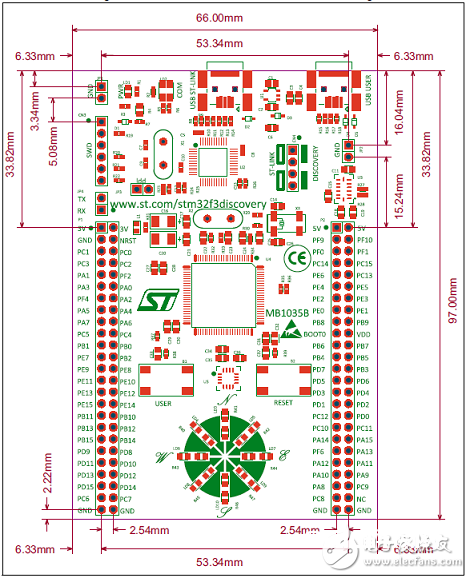
图11.Discovery kit STM32F3DISCOVERY PCB尺度图
概况请见:
https://www.st.com/content/ccc/resource/technical/document/user_manual/8a/56/97/63/8d/56/41/73
/DM00063382.pdf/files/DM00063382.pdf/jcr:content/translations/en.DM00063382.pdf
en.DM00063382.pdf