文章转自ADI官网,版权归属原作者一切
Introduction
With more than two billion microphones sold each year, the microphone market is of interest by virtue of its volume. about half of that market is for very inexpensive, low-grade microphones for the toy market and other applications where size and performance are not critical parameters. The rest of the volume is in portable, high-end applications, such as mobile phones, headsets, digital cameras, laptops, etc. The largest players in that market are mobile-phone manufacturers, who use some 900 million devices per year. At a projected annual growth rate of 10%, mobile phones constitute the fastest-growing segment of the microphone market. Mobile phones are getting smaller while incorporating a larger number of features, calling for next-generation microphones capable of increased performance.
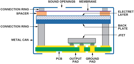
For many years, microphones used in telecom applications have been of the electret condenser (ECM) type. The microphone comprises a membrane, a back plate, and an electret layer. The movable membrane and fixed back plate are the plates of a variable capacitor. The electret layer stores a fixed charge corresponding to a capacitor voltage of approximately 100 V. Sound pressure will cause the membrane to move, varying the capacitance of the microphone. Since charge on the capacitor is constant, the voltage across the capacitor will vary with the changing capacitance, based on the formula for charge on a capacitor:

Q is the charge, in coulombs, C is the capacitance, in farads, and V is the voltage, in volts. The minuscule increases and decreases in capacitance, ΔC, with sound pressure, cause proportional decreases and increases in voltage, ΔV.

Microphones for mobile applications are quite small, typically 3 mm to 4 mm in diameter and 1 mm to 1.5 mm in thickness. Consequently, their capacitance is also relatively small. Typical values are of the order of 3 pF to 5 pF, and in some cases, as little as 1 pF.
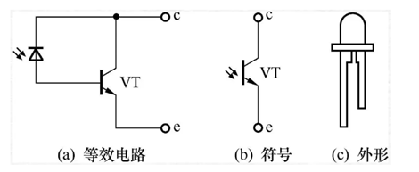
Having no drive strength, the signal produced by a capacitive microphone needs a buffer/amplifier prior to further processing. Conventionally this microphone preamplifier has been implemented using a simple junction field-effect transistor (JFET). Figure 1 shows a cross-section of a packaged JFET-based ECM.
As micromachining of electret microphones has improved, microphones have become smaller, and their element capacitance has decreased. Standard JFETs no longer suffice because their relatively large input capacitance significantly attenuates the signal from the microphone cartridge element. Fortunately, improvements in CMOS process technologies have led to improvements in amplifier circuits. Much is gained by replacing JFET-based amplifiers with CMOS analog and digital circuitry. Preamplifiers implemented in modern submicron CMOS processes have enabled, and will further enable, a wide range of improvements over traditional JFETs:
- Lower harmonic distortion
- Easier gain setting
- Multiple functional modes, including sleep mode for low power consumption
- Analog-to-digital conversion, enabling microphones with direct digital output
- Greatly enhanced sound quality
- Higher noise immunity
Digital-Output Microphone Preamplifier
Simple JFET-based amplifiers have inherently low power consumption, but they suffer from poor linearity and low accuracy. Thus, the main goal of improved microphone design is to combine preamplification with digital technology, increasing dynamic range through improved linearity and lower noise, while retaining very low power consumption.
Mobile phones present an inherently noisy environment. A drawback of the traditional JFET (and indeed any purely analog) solution is that analog microphone output signals can easily be corrupted by interfering signals creeping in between the amplifier and the analog-to-digital converter. Thus, incorporating analog-to-digital conversion into the microphone itself provides a digital output that is inherently less prone to corruption by interferers.
System Description
A block diagram of an integrated digital-output preamplifier and its interface is shown in Figure 2. The microphone-element signal is first amplified, and is then converted to digital by the analog-to-digital converter. These blocks receive their power from an internal regulated supply, ensuring good power supply rejection and an independent supply for the analog portion of the device.
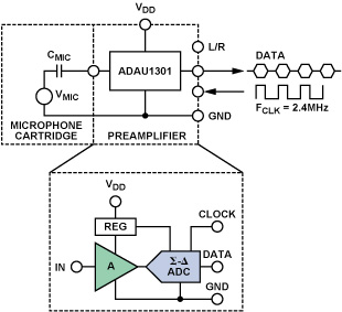
The preamplifier is built in CMOS using two operational transconductance amplifiers (OTAs) in an instrumentation-amplifier configuration where the gain is set using matched capacitors. This configuration, with its MOS input transistors, presents a highly desirable near-zero input admittance to the capacitive signal source. The use of capacitors for gain setting allows high gain accuracy—limited only by process lithography—and the inherently high linearity of poly-poly capacitors. The gain of the amplifier is easily set by metal-mask programming, allowing gains of up to 20 dB. The analog-to-digital converter is a fourth-order, single-loop, single-bit Σ-Δ modulator, whose digital output is a single-bit oversampled signal. Using a Σ-Δ modulator for analog-to-digital conversion offers several advantages:
- Noise shaping shifts the quantization noise upwards, pushing much of it outside of the band of interest. Thus, high accuracy can be obtained without imposing severe matching requirements for the circuitry.
- The analog-to-digital converter uses a single-bit Σ-Δ modulator, thus making it inherently linear.
- only one of the integrators in a single-bit, single-loop modulator requires severe design constraints. The inner-loop integrators, which have their outputs noise-shaped, have relaxed design requirements. This leads to lower power consumption.
A potential problem with higher-order Σ-Δ modulators is that they are prone to instability when the input exceeds the maximum stable amplitude (MSA). Higher-order modulators (>2) fail to return to stable operation when they become unstable due to overload, even when the input is reduced below the MSA. To counter potential instability, a digitally controlled feedback system alters the Σ-Δ noise transfer function, forcing the modulator back into stable operation.
A power-down mode, entered by allowing the system input clock frequency to drop below 1 kHz, lowers the current drawn by the system from 400 μA to approximately 50 μA, allowing the user to conserve power whenever the microphone is not needed. The start-up time from power-down is only 10 ms.
As a failure analysis feature, a special test mode enables access to various internal nodes in the circuit. A special preamble at the DATA pin during startup allows the failure analysis engineer access by switching these nodes to the DATA pin.
Noise Considerations
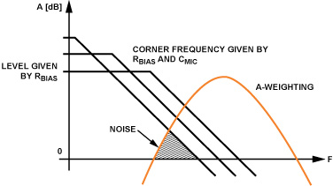
Three dominant noise sources in CMOS preamplifiers for capacitive microphones are flicker (1/f) noise, wideband white noise from the input transistors, and low-pass-filtered white noise from an input bias resistor, RBIAS, needed for setting the amplifier’s dc operating point. A-weighting is applied to take into account the human ear’s insensitivity to low frequencies.
Flicker-noise spectral density has an inverse dependency on transistor area; its magnitude, referred to the input, is given by
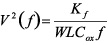
where Kf is a process-dependent constant, f is frequency, W is the MOS width, L its length and Cox is the gate capacitance per unit area. The 1/f-noise amplitude can be reduced by increasing the size of the input transistors. The input-referred white noise is inversely proportional to the transconductance, gm, of the metal-oxide-semiconductor transistor (MOST)

where k is Boltzmann’s constant and T is absolute temperature. For a MOST in strong inversion, gm≈ 2Id/Veff, where Id is the drain current, and the effective voltage, Veff = Vgs – Vth, the gate-to-source voltage minus the MOST threshold voltage, Vth. By designing the input pair to be very wide, a bipolar-like mode of operation is imposed upon the MOST as it enters the weak inversion operating mode. Here, gm = Id/(nVT), where n is the slope factor (typically 1.5) and VT is the thermal voltage. Thus, optimum white noise performance is achieved by maximizing the MOST aspect ratio.
The input bias resistor is connected to a capacitive source, so its noise will be low-pass filtered. Assuming that the noise is low-pass filtered white noise and the cutoff frequency is much smaller than the audio-band frequencies, it can be shown that the total noise power is kT/C, where C is the capacitance connected to the node.
As a consequence of the trend toward smaller microphone cartridges with lower cartridge capacitance, this noise source will increase as the microphone cartridge capacitance decreases. However, the audio-band noise power generated by the bias resistor will also depend on the cutoff frequency of the low-pass filter. The lower the cutoff frequency, the smaller the amount of the total noise power remaining in the audio frequency range. In order to keep the noise low, the value of the bias resistance will have to be increased by a factor of four for each halving of the microphone capacitance. For a 3-pF to 5-pF microphone capacitor, the resistor should have a minimum value of approximately 10 gigaohm.
A good solution for implementing such large value resistors on chip is a pair of antiparallel diodes which have a very large resistance around equilibrium, typically 1 teraohm to 10 teraohms. The resistance decreases for larger signals, assuring fast settling after overload situations. Figure 3 shows the in-band noise as a function of RBIAS.
The area of the input transistors of the preamplifier must be optimized in relation to the microphone capacitance. Although, as noted earlier, the 1/f noise will decrease if the input devices are made very large, the capacitive loading of the signal source will increase, attenuating the signal and reducing the wideband signal-to-noise ratio (SNR). This presents a trade-off: If the input device is made very small, the capacitive loading of the signal source becomes insignificant, but the 1/f noise increases dramatically, reducing low-frequency SNR. The optimum for maximizing SNR with respect to 1/f noise exists where the gate-source capacitance of the input device equals the microphone capacitance plus parasitic capacitance. The optimum for white noise exists where the gate-source capacitance of the input device equals one-third of the microphone capacitance plus parasitics. In practice, the best compromise is for the gate capacitance to fall between the two values.
Bootstrapping minimizes the input pad contribution to the overall chip input capacitance. As the output-referred white noise is proportional to gm, all current-source MOSTs are biased in the strong inversion region, ensuring minimum noise contribution.
Table 1 shows the key characteristics and performance of the ADAU1301 microphone preamplifier.
Table 1. Typical (Unless Noted) Characteristics and Performance of the ADAU1301
| Parameter | Value | Comments |
| Power Supply | 1.64 V to 3.65 V | Functional over full range, but specified performance is at 1.8 V |
| Supply Current | 400 µA | @ VDD = 1.8 V |
| Max Gain Variation | X ± 0.4 dBFS/VPeak | X is the specified gain |
| Max Lower Signal Bandwidth Limit | 25 Hz | |
| Min Upper Signal Bandwidth Limit | 20 kHz | |
| Equivalent Input-Referred Noise Level | 5 µV rms | A-weighted |
| Signal-to-Noise Ratio | 60.6 dBFS | Calculated at –27 dBFS/Pa microphone sensitivity |
| Dynamic Range | >86 dB | @ THD = 10%, dependent on gain |
| Input Capacitance | 0.1 pF | |
| Min Input Resistance | 15 gigaohm | |
| Start-Up Period | 500 ms | Measured from time when VDD becomes 1.8 V to time when the ASIC gain settles within 1 dB of its final settled value |
| Max Wake-Up Period | 10 ms | |
| Clock Frequency | 1 MHz to 4 MHz | Nominal Fclk = 2.4 MHz |
| Clock Duty Cycle fDC | 40% to 60% |
Toward a Fully Integrated Digital Microphone
This digital-output amplifier fulfills the needs of ECM elements, but the combination is not fully suitable for the emerging MEMS microphone market, which will require a higher degree of integration. Since the equivalent of an electret layer does not exist among solid-state MEMS elements, the capacitive element requires an integrated high-voltage source for bias. Because the microphone element constitutes a purely capacitive load, drawing no current from the biasing reference, an extended version of this amplifier system would include a low-power on-chip charge pump, obviating the need for a stored-charge source.
Conclusion
A microphone preamplifier created for the mobile microphone market enables and naturally leads to the digital-output microphone. Thorough noise analysis yields an instrumentation preamplifier with low noise that attains the desired dynamic range. The low-power Σ-Δ analog-to-digital converter achieves high resolution without imposing severe design constraints. A power-down mode provides maximum battery life by conserving power when the microphone is not needed. A special test mode, designed to give the manufacturer easy access to otherwise unreachable nodes for testing, has the added benefit of making the preamplifier’s analog output available for inspection.