文章转自ADI官网,版权归属原作者一切
Global demand for communication services continues to rise, and manufacturers must constantly reduce the size and cost of newly installed network equipment, while holding to high standards of service and quality. Part of building a robust network is managing clocks. Clock and timing requirements range from system-level synchronization of wired and wireless network hubs, to local signal distribution inside high density transceiver cabinets. To meet this wide array of design challenges, companies employ signal integrity experts to interpret specifications, oversee testing, and recommend components guaranteed to maintain clean, low jitter clocks throughout the network.
Ask any signal integrity expert about time jitter, and he/she is likely to outline the challenges posed by distributed components, which one-by-one, eat into the system’s total jitter budget. Time jitter on clocks is a measure of edge uncertainty. All systems can tolerate some amount of clock edge uncertainty. But when clock edges occur at increasingly random times, the system begins to break down. Missing one clock cycle may result in transmitters and receivers getting out of sync.
When time jitter limits a system’s overall signal-to-noise ratio or bit error rate, data may be lost. In a mobile network, this can lead to reduced call quality, or even dropped calls.
Consider a system that requires four clock functions in series: frequency multiplication, frequency division, phase offset, and level translation. If each function is performed by a separate component, the time jitter of each device must be mathematically combined to calculate the total clock path jitter. Four cascaded components, each with a jitter specification of 1.5 picoseconds (ps) rms, yield a total jitter of 3 ps rms (note: the square root of the sum of squares approach applies).
Therefore, the complete clock path has twice the jitter of individual components.
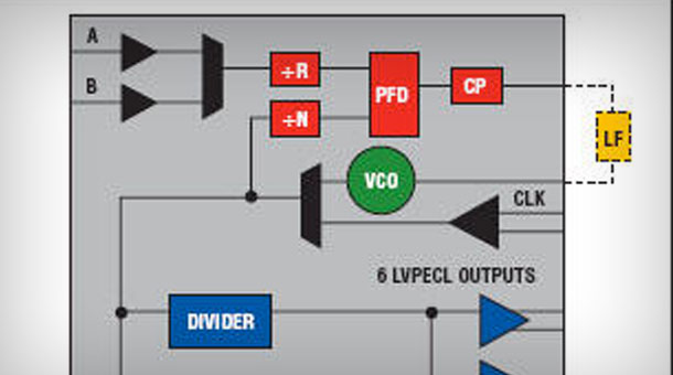
Now compare this to a solution where all critical timing functions are integrated into a single device—a complete phase-locked loop (PLL), including the voltage controlled oscillator (VCO) for frequency multiplication, five channel dividers with built-in phase offset capability, and clock output drivers offering the choice of LVPECL, LVDS, or CMOS levels. With the integrated approach, total clock path jitter may be controlled to well below 1 ps rms.
Analog Devices’ AD9516 integrated 2.8 GHz clock generator with 14-channel distribution enables network designers to generate 14 clean, low jitter clocks from a single chip. In addition, the AD9516 offers low time skew between its six LVPECL outputs. This capability means that designers are assured that all six clock edges occur within a well-defined time window. The LVDS/CMOS channels include programmable delay lines which may be used to compensate for delays in other parts of the system. Two inputs—A and B—feature automatic switchover, providing protection in the event of reference clock failure. Finally, because standalone oscillators are one of the most likely components to fail in a network, the AD9516 improves overall system reliability by integrating the VCO on-chip.
Analog Devices offers a wide range of clock and timing solutions that enable signal integrity engineers to maintain performance while reducing the size and cost of new equipment. For data sheets, free samples, and more information, visit www.analog.com/clock-timing/AD9516.