电路才能测验-1:直流电源交流电路
Circuit Knowledge Test-1: DC-DC Switching Regulator
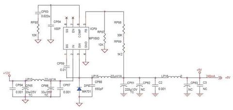
- If MP1580 switching frequency set at 400 KHz, and DC regulator output 5V, then please plot the switching wave-shape at IC pin-3 with line input 12V and 16V.假定MP1580作业在400 KHz,且稳压输出为5V,画出输入电压分别为12V 及 16V时,IC pin-3的正确波形。
- Now the DC regulated output is 5V. If we want to change the DC regulated output to 9V, what value of RP86 and RP89 are suitable for this change.现在的直流稳压输出为5V,假如期望提升为9V输出,怎么修正RP86 及 RP89的数值。
- Explain the charge and discharge functions of MA701, LP15, CP61 components in details. 阐明MA701, LP15, CP61元件的冲放电功用。
- According to MP1580 switching efficiency chart da
ta: DC 12V input and DC 5V 240mA output will display 85% efficiency. What input current rating will be for 12V supply? 依据MP1580的规格书,当直流12V输入,输出为5V 240mA时,转化功率为85%,核算输入电流值。
- Same condition as the Question-4: If MP1580 IC with SOP-8 package dissipation 160°C/W, then what surface temperature will be for MP1580 at 25°C room temperature?同上第四题,MP1580选用SOP-8包装的传热系数为160°C/W,核算其室温25°C时的IC表面温度。
- What is the maximum allowable ripple voltage at 5V DC regulated output to assure 40 db S/N if this 5V will supply for a video function IC? 当直流稳压输出5V,用来供给印象电路时,为了保证到达40 db S/N,求其最大容许连波电压数值。
- Explain the function of CP59, LP17, LP16 components? 阐明CP59, LP17, LP16元件的功用。
试题回答
Circuit Knowledge Test-1: DC-DC Switching Regulator
ANS-1:

ANS-2:
RP86=62K, RP89=1K8.
(R86+R89+R87)/R87 = 5.0/Vref then Vref=5.0/4.12=1.22
RN86+RN89 = (9.0/Vref * R87) –R87 = 63.8K (62K + 1K8)
RP86=62K, RP89=1K8.
ANS-3:
Switching pulse comes from ICP9 pin-3 and charge through LP15 to CP61 during switching-on duty-cycle. The inductive voltage across LP15 will then charge through DP8 to CP61 during switching-off duty-cycle. (Note that inductive current will produce reverse voltage across coil LP15)
ANS-4:
120 mA
DC input power = 5 * 0.24 / 0.85 = 1.41 W then DC input current = 1.41/12 = 120 mA.
ANS-5:
58.6 °C
Power loss = 1.41-1.2 = 0.21 W then Thermal heat rise Tht = 160 * 0.21 = 33.6 °C
Final junction temperature Tj = 25 + 33.6 = 58.6 °C
ANS-6:
50 mVpp.
Because 40 db means 1% level, then 5 Volt d-c on
ANS-7:
CP59: Boot-straping capacitor for driving output power FET.
LP17: Filter choke for filtering switching pulse generated from %&&&&&%P9.
LP16: Filter choke for filtering switching noise to reach 40 db noise limit.