latTIce公司的iCE40系列是超低功耗非易式FPGA器材,查找表(LUT)从384到7680.此外还具有嵌入区RAM(EBR),非易失可装备存储器(NVCM)和锁相环(PLL),十分适用在低成本量大的消费类和体系使用.本文介绍了iCE40系列首要特性和iCE40LP/HX 1K器材架构图,以及iCE40 16-WLCSP评价板首要特性,电路图和资料清单.
The iCE40 family of ultra-low power, non-volaTIle FPGAs has five devices with densiTIes ranging from 384 to 7680 Look-Up Tables (LUTs). In addiTIon to LUT-based, low-cost programmable logic, these devices feature Embedded Block RAM (EBR), Non-volatile Configuration Memory (NVCM) and Phase Locked Loops (PLLs). These features allow the devices to be used in low-cost, high-volume consumer and system applications. Select packages offer High-Current drivers that are ideal to drive three white LEDs, or one RGB LED. The iCE40 devices are fabricated on a 40 nm CMOS low power process. The device architecture has several features such as programmable low-swing differential I/Os and the ability to turn off on-chip PLLs dynamically. These features help manage static and dynamic power consumption, resulting in low static power for all members of the family.
The iCE40 devices are available in two versions – ultra low power (LP) and high performance (HX) devices. The iCE40 FPGAs are available in a broad range of advanced halogen-free packages ranging from the space saving 1.40×1.48mm WLCSP to the PCB-friendly 20×20 mm TQFP. Table 1-1 shows the LUT densities, package and I/O options, along with other key parameters. The iCE40 devices offer enhanced I/O features such as pull-up resistors. Pull-up features are controllable on a “per-pin” basis.
The iCE40 devices also provide flexible, reliable and secure configuration from on-chip NVCM. These devices can also configure themselves from external SPI Flash or be configured by an external master such as a CPU. Lattice provides a variety of design tools that allow complex designs to be efficiently implemented using the iCE40 family of devices. Popular logic synthesis tools provide synthesis library support for iCE40. Lattice design tools use the synthesis tool output along with the user-specified preferences and constraints to place and route the design in the iCE40 device. These tools extract the timing from the routing and back-annotate it into the design for timing verification. Lattice provides many pre-engineered IP (Intellectual Property) modules, including a number of reference designs, licensed free of charge, optimized for the iCE40 FPGA family. By using these configurable soft core IP cores as standardized blocks, users are free to concentrate on the unique aspects of their design, increasing their productivity.
iCE40系列首要特性:
Flexible Logic Architecture
• Five devices with 384 to 7,680 LUT4s and 10 to 206 I/Os
Ultra Low Power Devices
• Advanced 40 nm low power process
• As low as 21 μA standby power
• Programmable low swing differential I/Os
Embedded and Distributed Memory
• Up to 128 Kbits sysMEM™ Embedded Block RAM
Pre-Engineered Source Synchronous I/O
• DDR registers in I/O cells
High Current LED Drivers
• Three High Current Drivers used for three differ-ent LEDs or one RGB LED
High Performance, Flexible I/O Buffer
• Programmable sysIO™ buffer supports wide range of interfaces:
– LVCMOS 3.3/2.5/1.8
– LVDS25E, subLVDS
– Schmitt trigger inputs, to 200 mV typical hysteresis
– Standard SPI Interface
– Internal Nonvolatile Configuration Memory (NVCM)
– As small as 1.40×1.48mm
• Programmable pull-up mode
Flexible On-Chip Clocking
• Eight low-skew global clock resources
• Up to two analog PLLs per device
Flexible Device Configuration
• SRAM is configured through:
Broad Range of Package Options
• WLCSP, QFN, VQFP, TQFP, ucBGA, caBGA, and csBGA package options
• Small footprint package options
• Advanced halogen-free packaging
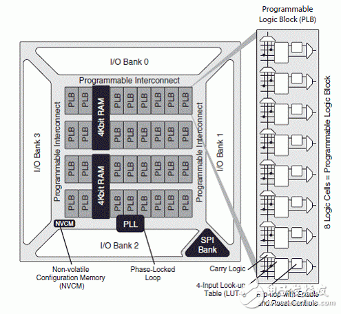
图1. iCE40LP/HX 1K器材架构图
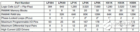
iCE40系列首要性能表:
iCE40 16-WLCSP评价板
The iCE40 16-WLCSP Evaluation Kit is a low-cost, feature-rich evaluation platform to help you evaluate and develop with the iCE40LP1K FPGA in the 16-WLCSP package. One key feature is the RGB LED control capability. With the evaluation kit and the available RGB LED GUI, you have complete control over the LED. You can control the color, brightness, blinking and breathing rate of the RGB LED. The GUI is available for a PC with Windows or a MAC.
iCE40 16-WLCSP评价板首要特性:
The iCE40 16-WLCSP Evaluation Kit includes:
• iCE40 16-WLCSP Evaluation Board – The ICE40 16-WLCSP Evaluation Board features the following on-board components and circuits:
– iCE40 (iCE40LP1K-SWG16) device in a 16-ball WLCSP package.
– Example of a board using this 0.35-pitch WLCSP package.
– High-current LED output – Infrared transmit
– Barcode emulation
– 27MHz oscillator
– iCE40 Current Measurements
– Standard USB cable for device programming
– RoHS-compliant packaging and process
• Pre-loaded Demo – The kit includes a pre-loaded demo to control the onboard RGB LED in conjunction with a software run GUI.
• USB Connector Cable – A mini B USB port provides power, a programming interface and communication for the software RGB LED GUI to the ICE40 SPI port.
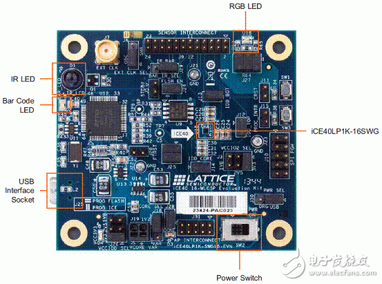
图2. iCE40 16-WLCSP评价板外形图
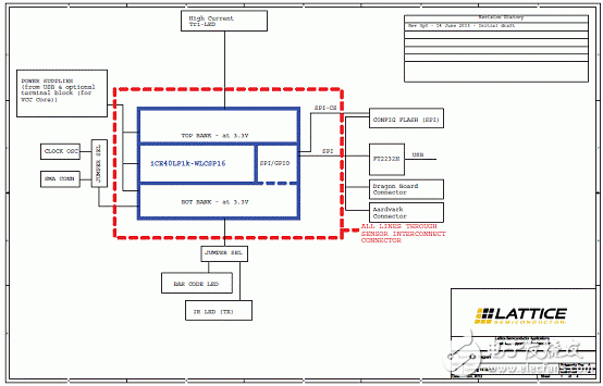
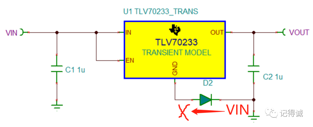
图3. iCE40 16-WLCSP评价板电路图(1)
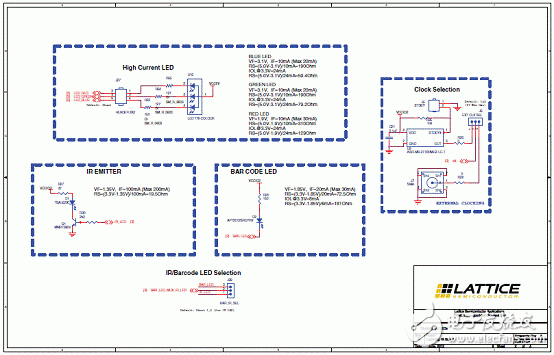
图4. iCE40 16-WLCSP评价板电路图(2)
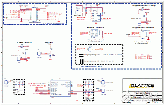
图5. iCE40 16-WLCSP评价板电路图(3)
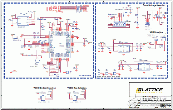
图6. iCE40 16-WLCSP评价板电路图(4)
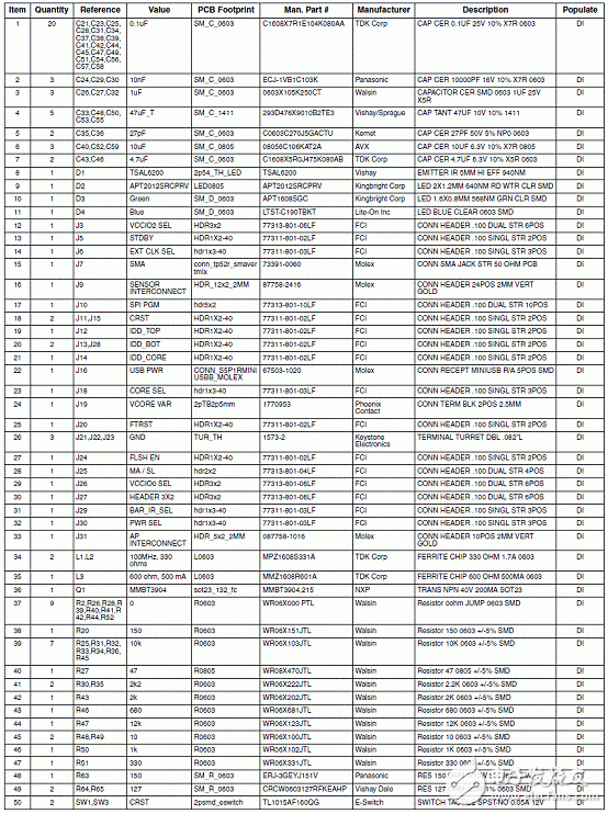
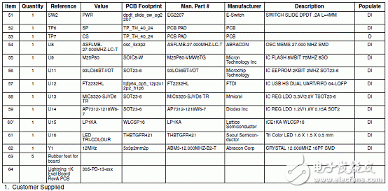
iCE40 16-WLCSP评价板资料清单: