文章转自ADI官网,版权归属原作者一切
In consumer electronic applications, which tend to be lower in frequency and less demanding than typical clock buffering applications, inexpensive high-speed op amps (~100 MHz bandwidth) can offer an attractive alternative to traditional clock buffers. High-speed amplifiers can be less expensive than traditional clock buffers, yet they can accommodate a wide range of design configurations.
The ADA4850 (-1/-2), ADA4851 (-1/-2/-4), ADA4853 (-1/-2/-3) and AD8061 single-supply op amps are excellent choices for low-cost clock buffers. These amplifiers all feature low supply voltage, low supply current, a power-down mode for power sensitive applications, and rail-to-rail outputs, which enable wide dynamic range.
One advantage of an op amp versus a traditional clock buffer is flexibility. Op amps allow clock pulses to be buffered, amplified, offset, inverted, summed, subtracted or filtered. They provide high input impedance, low input bias current, low supply current, independent power-down (for multiple amplifiers in a single package), low output impedance, and low propagation delay.
Designers must recognize and adhere to some operating constraints when using op amps in clock buffer applications. For example, voltage feedback amplifiers specify a gain bandwidth product. As the closed-loop gain of the amplifier circuit increases, its bandwidth decreases. Large gains therefore mean less bandwidth. Cascading multiple amplifers, each with lower gain, allows the amplifier to operate at a higher bandwidth, preserving the overall gain and bandwidth of the signal path.
Single-supply operation is important for portable electronics. By definition, the input common-mode range of a single-supply op amp includes the negative rail (ground); most can go 200 mV below ground. This doesn’t mean that the output can swing below ground, however. The output stage of a typical bipolar rail-to-rail amplifier uses a common emitter configuration. Therefore, the closest the output can come to the rail is Vce (sat), which can range from tens of millivolts to hundreds of millivolts, depending on the output load.
Fortunately, in these applications, the output does not usually have to swing all the way to ground. When the input gets too close to ground, however (around 100 mV – 200 mV), the output stage can saturate, introducing distortion and long recovery times. In dc-coupled systems, keep the “low” of the signal above 200 mV or use a –200 mV negative supply voltage. Either method will prevent the output stage from going into saturation.
Amplifiers also specify headroom, or how close they can swing to the positive rail, so care must also be taken to address the high side of the input common-mode range as well. If the input voltage gets too high, the input stage will distort and cut off. The ADA4850 and ADA4851 require 2.2 V of headroom, the AD8061 requires 1.8 V, and the ADA4853 requires only 1.2 V.
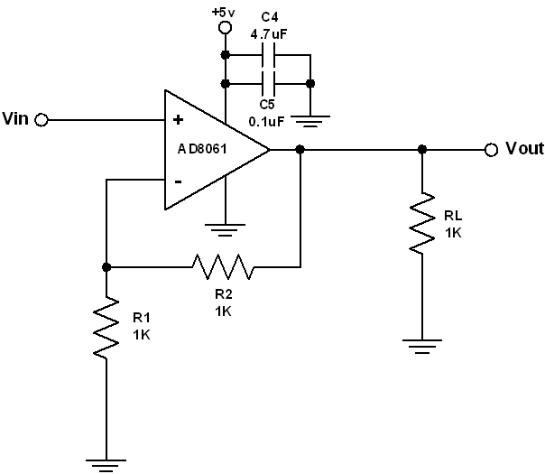
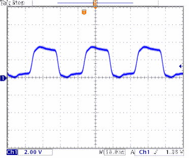
Figure 1 shows a single-supply non-inverting op amp clock buffer with a gain of +2. Figure 2 shows its transient response. As configured, the upper limit for the AD8061 is about 33 MHz. Its 2-ns propagation delay is comparable to some dedicated clock buffers.
In some applications, ac coupling can be used, allowing higher bandwidth amplifiers to be used for extended frequency performance. These amplifiers can be used in single-supply applications by biasing the amplifier inputs and outputs to mid-supply.
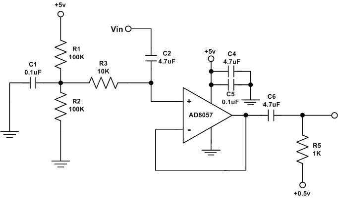
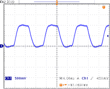
Figure 3 shows a schematic using the AD8057 high-speed amplifier. Featuring 325-MHz bandwidth and 1150 V/μs slew rate, it is configured for unity gain. Note that the load resistor is returned to a voltage that is the dc average of the input signal. This ensures that the output will be referenced back to ground. The upper operating range of this configuration is approximately 100 MHz. Figure 4 shows the clock response. Note that good pulse fidelity is maintained at 90 MHz.
As shown, when a design calls for a clock buffer, a high-speed amplifier can often provide more flexibility at lower cost, enabling high-speed amplifiers to compete with traditional clock buffers in many applications. Either single- or dual-supply amplifiers can be used, depending upon the specific application.