Xilinx(赛灵思)公司的轿车(XA)电子操控单元(ECU)开发套件是根据赛灵思公司满意轿车使用规范的低本钱Xilinx® XA Spartan-3E 现场可编程门阵列(FPGA)器材。XA 轿车 ECU套件为快速开发车内网络、信息文娱、辅佐驾驭以及驾驭信息体系供给了一个渠道。它该套件包含一个带有预工程化硬件接口的开发板,支撑很多轿车使用IP。使用这一完好的开发环境,轿车规划人员可快速完结器材评价,敏捷完结规划并开端运转。本文介绍了Xilinx的Spartan-3E FPGA系列首要性能,以及轿车电子ECU 开发套件 (HW-XA3S1600E-UNI-G)的首要性能和方框图。
赛灵思轿车(XA)电子操控单元(ECU)开发套件是根据赛灵思公司满意轿车使用规范的低本钱Xilinx® XA Spartan-3E 现场可编程门阵列(FPGA)器材。XA 轿车 ECU套件为快速开发车内网络、信息文娱、辅佐驾驭以及驾驭信息体系供给了一个渠道。
XA轿车ECU开发套件。该套件包含一个带有预工程化硬件接口的开发板,支撑很多轿车使用IP。使用这一完好的开发环境,轿车规划人员可快速完结器材评价,敏捷完结规划并开端运转。
XA 轿车 ECU开发套件供给了开发完好子体系所需求的一切元器材,包含配有一片XA Spartan-3E 160万体系门FPGA的XA1600E开发板,板上硬件接口,如CAN 2.0B 和 C、Ethernet 10/100、USB 2.0、SPI 和 SCI。预先验证的赛灵思和第三方使用IP为开发MOST® 体系、FlexRay 衔接以及高速和低速CAN总结接口供给了必要的构建模块。该套件还包含一个带有通用适配器的电源、编程和定制串行电缆、快速入门攻略以及包含便利评价的参阅规划的资源CD。一起还支撑赛灵思嵌入式开发套件和ISE规划东西评价版。
关于XA Spartan-3E FPGA
XA Spartan-3E FPGA系列满意大批量本钱灵敏轿车电子使用要求。该系列的五款器材供给从10万至160万体系门不同密度和不同封装组合。XA器材一起供给扩展温度规模Q-Grade (-40°C 至 +125°C Tj) 和 I-Grade (-40°C 至 +100°C Tj)器材,而且契合业界公认的AEC-Q100规范。与此前的器材比较,这些90nm器材单位美元本钱供给了更多功用和I/O带宽,在可编程逻辑职业确立了新规范。因为其超低本钱,XA Spartan-3E FPGA供给了优异的代替处理计划,避免了ASIC和ASSP的高掩膜本钱和长开发周期。
一.Spartan-3E FPGA系列
The Spartan-3E family of Field-Programmable Gate Arrays (FPGAs) is specifically designed to meet the needs of high volume, cost-sensitive consumer electronic applications.
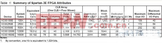
The five-member family offers densities ranging from 100,000 to 1.6 million system gates.The Spartan-3E family builds on the success of the earlier Spartan-3 family by increasing the amount of logic per I/O, significantly reducing the cost per logic cell. New features improve system performance and reduce the cost of configuration.
These Spartan-3E enhancements, combined with advanced 90 nm process technology, deliver more functionality and bandwidth per dollar than was previously possible, setting new standards in the programmable logic industry.
Because of their exceptionally low cost, Spartan-3E FPGAs are ideally suited to a wide range of consumer electronics applications, including broadband access, home networking, display/projection, and digital television equipment.
The Spartan-3E family is a superior alternative to mask programmed ASICs. FPGAs avoid the high initial cost, the lengthy development cycles, and the inherent inflexibility of
conventional ASICs. Also, FPGA programmability permits design upgrades in the field with no hardware replacement necessary, an impossibility with ASICs.
Spartan-3E FPGA系列首要特性:
Very low cost, high-performance logic solution for high-volume, consumer-oriented applications
Proven advanced 90-nanometer process technology
Multi-voltage, multi-standard SelectIO interface pins
– Up to 376 I/O pins or 156 differential signal pairs
– LVCMOS, LVTTL, HSTL, and SSTL single-ended signal standards
– 3.3V, 2.5V, 1.8V, 1.5V, and 1.2V signaling
– 622+ Mb/s data transfer rate per I/O
– True LVDS, RSDS, mini-LVDS, differential HSTL/SSTL differential I/O
– Enhanced Double Data Rate (DDR) support
– DDR SDRAM support up to 333 Mb/s
Abundant, flexible logic resources
– Densities up to 33,192 logic cells, including optional shift register or distributed RAM support
– Efficient wide multiplexers, wide logic
– Fast look-ahead carry logic
– Enhanced 18 x 18 multipliers with optional pipeline
– IEEE 1149.1/1532 JTAG programming/debug port
Hierarchical SelectRAM memory architecture
– Up to 648 Kbits of fast block RAM
– Up to 231 Kbits of efficient distributed RAM
Up to eight Digital Clock Managers (DCMs)
– Clock skew elimination (delay locked loop)
– Frequency synthesis, multiplication, division
– High-resolution phase shifting
– Wide frequency range (5 MHz to over 300 MHz)
Eight global clocks plus eight additional clocks per each half of device, plus abundant low-skew routing
Configuration interface to industry-standard PROMs
– Low-cost, space-saving SPI serial Flash PROM
– x8 or x8/x16 parallel NOR Flash PROM
– Low-cost Xilinx Platform Flash with JTAG
Complete Xilinx ISE and WebPACK development system support
MicroBlaze and PicoBlaze embedded processor cores
Fully compliant 32-/64-bit 33 MHz PCI support (66 MHz in some devices)
Low-cost QFP and BGA packaging options
– Common footprints support easy density migration
– Pb-free packaging options
二.轿车电子ECU 开发套件 (HW-XA3S1600E-UNI-G)
The Automotive ECU Development Kit (HW-XA3S1600E-UNI-G) is a configurable and extensible platform suited for a wide range of automotive applications right out of the box.
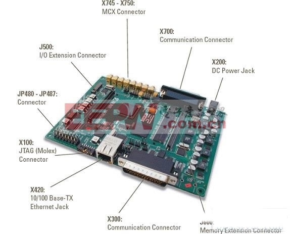
图1。轿车电子ECU 开发套件外形图
With its small form factor, it can be easily placed in standard metal housing. The board was designed to be powered by a 12-volt power supply for in-vehicle prototype use. Powered by a completely field-configurable Spartan-3E FPGA platform, this kit:
Combines programmable logic for custom driven IP applications with the Xilinx MicroBlaze32-bit microprocessor core.
Features robust memory subsystem containing on-board Flash and SRAM memory.
Supports standard Automotive and System-on-chip peripherals including all necessary physical layers on board the ECU, such as JTAG, 10/100 Ethernet, USB 2.0, 12-bit ADC, High and Low Speed CAN, FlexRay, LIN, K-Line, UART, SPI and over 150 user programmable I/Os.
ECU 开发套件包含:
XA1600E development board with the XC3S1600EFG484 device
Power supply with universal adaptor
Programming cable
Custom serial cable
QuickStart guide
EDK and ISE evaluation tools
Resource CD with reference designs for easy evaluation
ECU 开发套件首要特性:
Xilinx device: XC3S1600EFG484 FPGA
Complete out-of-the box development system
On-board hardware interfaces such as CAN 2.0C, Ethernet 10/100, USB 2.0, SPI, and SCI
Support for pre-verified Xilinx and Partner IP for High and Low Speed CAN, FlexRay and MOST® network interfaces.
Daughter card is required for MOST interface.
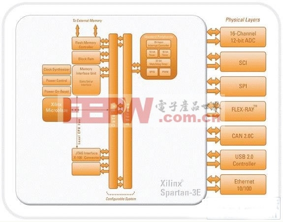
图2。ECU 开发板方框图