文章转自ADI官网,版权归属原作者一切
Introduction
All analog-to-digital converters (ADCs) have a certain amount of input-referred noise—modeled as a noise source connected in series with the input of a noise-free ADC. Input-referred noise is not to be confused with quantization noise, which is only of interest when an ADC is processing time-varying signals. In most cases, less input noise is better; however, there are some instances where input noise can actually be helpful in achieving higher resolution. If this doesn’t seem to make sense right now, read on to find out how some noise can be good noise.
Input-Referred Noise (Code-Transition Noise)
Practical ADCs deviate from ideal ADCs in many ways. Input-referred noise is certainly a departure from the ideal, and its effect on the overall ADC transfer function is shown in Figure 1. As the analog input voltage is increased, the “ideal” ADC (shown in Figure 1a) maintains a constant output code until a transition region is reached, at which point it instantly jumps to the next value, remaining there until the next transition region is reached. A theoretically perfect ADC has zero code-transition noise, and a transition region width equal to zero. A practical ADC has a certain amount of code transition noise, and therefore a finite transition region width. Figure 1b shows a situation where the width of the code transition noise is approximately one least-significant bit (LSB) peak-to-peak.

Internally, all ADC circuits produce a certain amount of rms noise due to resistor noise and “kT/C” noise. This noise, present even for dc input signals, accounts for the code-transition noise, now generally referred to as input-referred noise. Input-referred noise is most often characterized by examining the histogram of a number of output samples, while the input to the ADC is held constant at a dc value. The output of most high speed or high resolution ADCs is a distribution of codes, typically centered around the nominal value of the dc input (see Figure 2).
To measure the amount of input-referred noise, the input of the ADC is either grounded or connected to a heavily decoupled voltage source, and a large number of output samples are collected and plotted as a histogram (referred to as a grounded-input histogram if the input is nominally at zero volts). Since the noise is approximately Gaussian, the standard deviation of the histogram, σ, which can be calculated, corresponds to the effective input rms noise. See Further Reading 6 for a detailed description of how to calculate the value of σ from the histogram data. It is common practice to express this rms noise in terms of LSBs rms, corresponding to an rms voltage referenced to the ADC full-scale input range. If the analog input range is expressed as digital numbers, or counts, input values, such as σ, can be expressed as a count of the number of LSBs.
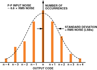
Although the inherent differential nonlinearity (DNL) of the ADC will cause deviations from an ideal Gaussian distribution (for instance, some DNL is evident in Figure 2), it should be at least approximately Gaussian. If there is significant DNL, the value of σ should be calculated for several different dc input voltages and the results averaged. If the code distribution is significantly non-Gaussian, as exemplified by large and distinct peaks and valleys, for instance—this could indicate either a poorly designed ADC or—more likely—a bad PC board layout, poor grounding techniques, or improper power supply decoupling (see Figure 3). Another indication of trouble is when the width of the distribution changes drastically as the dc input is swept over the ADC input voltage range.

Noise-Free (Flicker-Free) Code Resolution
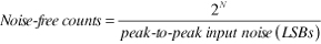
The noise-free code resolution of an ADC is the number of bits of resolution beyond which it is impossible to distinctly resolve individual codes. This limitation is due to the effective input noise (or input-referred noise) associated with all ADCs and described above, usually expressed as an rms quantity with the units of LSBs rms. Multiplying by a factor of 6.6 converts the rms noise into a useful measure of peak-to-peak noise—the actual uncertainty with which a code can be identified—expressed in LSBs peak-to-peak. Since the total range (or span) of an N-bit ADC is 2N LSBs, the total number of noise-free counts is therefore equal to:
 |
(1) |
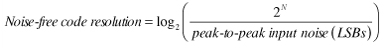
The number of noise-free counts can be converted into noise-free (binary) code resolution by calculating the base-2 logarithm as follows:
 |
(2) |
The noise-free code resolution specification is generally associated with high-resolution sigma-delta measurement ADCs. It is most often a function of sampling rate, digital-filter bandwidth, and programmable-gain-amplifier (PGA) gain (hence input range). Figure 4 shows a typical table—taken from the data sheet of the AD7730 sigma-delta ADC.
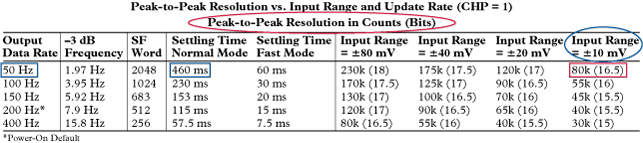
Note that for an output data rate of 50 Hz and an input range of ±10 mV, the noise-free code resolution is 16.5 bits (80,000 noise-free counts). The settling time under these conditions is 460 ms, making this ADC an ideal candidate for a precision weigh-scale application. Data of this kind is available on most data sheets for high-resolution sigma-delta ADCs suitable for precision measurement applications.
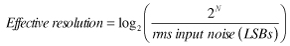
The ratio of the full-scale range to the rms input noise (rather than peak-to-peak noise) is sometimes used to calculate resolution. In this case, the term effective resolution is used. Note that under identical conditions, effective resolution is larger than noise-free code resolution by log2(6.6), or approximately 2.7 bits.
 |
(3) | |
 |
(4) |
Some manufacturers prefer to specify effective resolution rather than noise-free code resolution because it results in a higher number of bits—the user should check the data sheet closely to make sure which is actually specified.
Digital Averaging Increases Resolution and Reduces Noise
The effects of input-referred noise can be reduced by digital averaging. Consider a 16-bit ADC which has 15 noise-free bits at a sampling rate of 100 kSPS. Averaging two measurements of an unchanging signal for each output sample reduces the effective sampling rate to 50 kSPS—and increases the SNR by 3 dB and the number of noise-free bits to 15.5. Averaging four measurements per output sample reduces the sampling rate to 25 kSPS—and increases the SNR by 6 dB and the number of noise-free bits to 16.
We can go even further and average 16 measurements per output; the output sampling rate is reduced to 6.25 kSPS, the SNR increases by another 6 dB, and the number of noise-free bits increases to 17. The arithmetic precision in the averaging must be carried out to the larger number of significant bits in order to gain the extra “resolution.”
The averaging process also helps smooth out the DNL errors in the ADC transfer function. This can be illustrated for the simple case where the ADC has a missing code at quantization level k. Even though code k is missing because of the large DNL error, the average of the two adjacent codes, k – 1 and k + 1, is equal to k.
This technique can therefore be used effectively to increase the dynamic range of the ADC at the expense of overall output sampling rate and extra digital hardware. It should also be noted that averaging will not correct the inherent integral nonlinearity of the ADC.
Now, consider the case of an ADC that has extremely low input-referred noise, and the histogram shows a single code no matter how many samples are taken. What will digital averaging do for this ADC? This answer is simple—it will do nothing! No matter how many samples are averaged, the answer will be the same. However, as soon as enough noise is added to the input signal, so that there is more than one code in the histogram, the averaging method starts working again. Thus—interestingly—some small amount of noise is good (at least with respect to the averaging method); however, the more noise present at the input, the more averaging is required to achieve the same resolution.
Don’t Confuse Effective Number of Bits (ENOB) with Effective Resolution or Noise-Free Code Resolution
Because of the similarity of the terms, effective number of bits and effective resolution are often assumed to be equal. This is not the case.
Effective number of bits (ENOB) is derived from an FFT analysis of the ADC output when the ADC is stimulated with a full-scale sine-wave input signal. The root-sum-of-squares (RSS) value of all noise and distortion terms is computed, and the ratio of the signal to the noise-and-distortion is defined as SINAD, or S/(N+D). The theoretical SNR of a perfect N-bit ADC is given by:
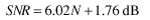 |
(5) |
ENOB is calculated by substituting the ADC’s computed SINAD for SNR in Equation 5 and solving equation for N.
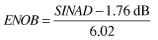 |
(6) |
The noise and distortion used to calculate SINAD and ENOB include not only the input-referred noise but also the quantization noise and the distortion terms. SINAD and ENOB are used to measure the dynamic performance of an ADC, while effective resolution and noise-free code resolution are used to measure the noise of the ADC under essentially dc input conditions, where quantization noise is not an issue.
Using Noise Dither to Increase an ADC’s Spurious-Free Dynamic Range
Spurious-free dynamic range (SFDR) is the ratio of the rms signal amplitude to the rms value of the peak spurious spectral component. Two fundamental limitations to maximizing SFDR in a high-speed ADC are the distortion produced by the front-end amplifier and the sample-and-hold circuit; and that produced by nonlinearity in the transfer function of the encoder portion of the ADC. The key to achieving high SFDR is to minimize both sources of nonlinearity.
Nothing can be done externally to the ADC to significantly reduce the inherent distortion caused by its front end. However, the differential nonlinearity in the ADC’s encoder transfer function can be reduced by the proper use of dither (external noise that is intentionally summed with the analog input signal).
Dithering can be used to improve SFDR of an ADC under certain conditions (see Further Reading 2–5). For example, even in a perfect ADC, some correlation exists between the quantization noise and the input signal. This correlation can reduce the SFDR of the ADC, especially if the input signal is an exact sub-multiple of the sampling frequency. Summing about 1/2-LSB rms of broadband noise with the input signal tends to randomize the quantization noise and minimize this effect (see Figure 5a). In most systems, however, the noise already riding on top of the signal (including the input-referred noise of the ADC) obviates the need for additional dither noise. Increasing the wideband rms noise level beyond approximately one LSB will proportionally reduce the SNR and result in no additional improvement.
Other schemes have been developed using larger amounts of dither noise to randomize the transfer function of the ADC. Figure 5b shows a dither-noise source comprising a pseudo-random-number generator driving a DAC. This signal is subtracted from the ADC input signal and then digitally added to the ADC output, thereby causing no significant degradation SNR. An inherent disadvantage of this technique, however, is that the input signal swing must be reduced to prevent overdriving the ADC as the amplitude of the dither signal is increased. Note that although this scheme improves distortion produced by the ADC’s encoder nonlinearity, it does not significantly improve distortion created by its front end.

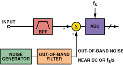
Another method, one that is easier to implement—especially in wideband receivers—is to inject a narrow-band dither signal outside the signal band of interest, as shown in Figure 6. Usually, no signal components are located in the frequency range near dc, so this low-frequency region is often used for such a dither signal. Another possible location for the dither signal is slightly below fS/2. The dither signal occupies only a small bandwidth relative to the signal bandwidth (usually a bandwidth of a few hundred kHz is sufficient), so no significant degradation in SNR occurs—as it would if the dither was broadband.
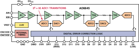
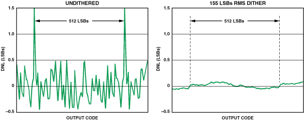
A subranging, pipelined ADC, such as the AD6645 14-bit, 105-MSPS ADC (see Figure 7), has very small differential nonlinearity errors that occur at specific code transition points across the ADC range. The AD6645 includes a 5-bit ADC (ADC1), followed by a 5-bit ADC2 and a 6-bit ADC3. The only significant DNL errors occur at the ADC1 transition points—the second- and third-stage DNL errors are minimal. There are 25 = 32 decision points associated with ADC1, which occur every 68.75 mV (29 = 512 LSBs) for a 2.2-V full-scale input range. Figure 8 shows a greatly exaggerated representation of these nonlinearities.

With an analog input up to about 200 MHz, the distortion components produced by the front end of the AD6645 are negligible compared to those produced by the encoder. That is, the static nonlinearity of the AD6645 transfer function is the chief limitation to SFDR.
The goal is to select the proper amount of out-of-band dither so that the effects of these small DNL errors are randomized across the ADC input range, thereby reducing the average DNL error. Experimentally, it was determined that making the peak-to-peak dither noise cover about two ADC1 transitions gives the best improvement in DNL. The DNL is not significantly improved with higher levels of noise. Two ADC1 transitions cover 1024 LSBs peak-to-peak, or approximately 155 (= 1024/6.6) LSBs rms.
The first plot shown in Figure 9 shows the undithered DNL over a small portion of the input signal range, including two of the subranging points, which are spaced 68.75 mV (512 LSBs) apart. The second plot shows the DNL after adding (and later filtering out) 155 LSBs of rms dither. This amount of dither corresponds to approximately –20.6 dBm. Note the dramatic improvement in the DNL.
Dither noise can be generated in a number of ways. For example, noise diodes can be used, but simply amplifying the input voltage noise of a wideband bipolar op amp provides a more economical solution. This approach, described in detail elsewhere (Further Reading 3, 4, and 5) will not be discussed here.
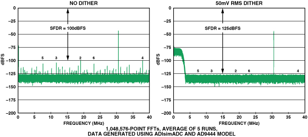
The dramatic improvement in SFDR obtainable with out-of-band dither is shown in Figure 10, using a deep (1,048,576-point) FFT, where the AD6645 is sampling a –35-dBm, 30.5-MHz signal at 80 MSPS. Note that the SFDR without dither is approximately 92 dBFS, compared to 108 dBFS with dither—a substantial 16-dB improvement!
The AD6645 ADC, introduced by Analog Devices in 2000, has until recently represented the ultimate in SFDR performance. In the few years since its introduction, improvements in both process technology and circuit design have resulted in even higher performance ADCs, such as the AD9444 (14 bits at 80 MSPS), AD9445 (14 bits, 105 MSPS and 125 MSPS speed grades), and the AD9446 (16 bits, 80 MSPS and 100 MSPS speed grades). These ADCs have very high SFDR (typically greater than 90 dBc for a 70-MHz, full-scale input signal) and low DNL. Still, the addition of an appropriate out-of-band dither signal can improve the SFDR under certain input signal conditions.
Figure 11 models FFT plots of the AD9444, with and without dither. It can be seen that, under the given input conditions, the addition of dither improves the SFDR by 25 dB. The data was taken using the ADIsimADC™ program and the AD9444 model.
Even though the results shown in Figures 10 and 11 are fairly dramatic, it should not be assumed that the addition of out-of-band noise dither will always improve the SFDR of the ADC under all conditions. We reiterate that dither will not improve the linearity of the front-end circuits of the ADC. Even with a nearly ideal front end, the effects of dither will be highly dependent upon both the amplitude of the input signal and the amplitude of the dither signal itself. For example, when signals are near the full-scale input range of the ADC, the integral nonlinearity of the transfer function may become the limiting factor in determining SFDR, and dither will not help. In any event, the data sheet should be studied carefully—in some cases dithered and undithered data may be shown, along with suggestions for the amplitude and bandwidth. Dither may be a built-in feature of newer IF-sampling ADCs.
Summary
In this discussion we have considered the input-referred noise, common to all ADCs. In precision, low-frequency measurement applications, effects of this noise can be reduced by digitally averaging the ADC output data, using lower sampling rates and additional hardware. While the resolution of the ADC can actually be increased by this averaging process, integral-nonlinearity errors are not reduced. only a small amount of input-referred noise is needed to increase the resolution by the averaging technique; however, use of increased noise requires a larger number of samples in the average, so a point of diminishing returns is reached.
In certain high speed ADC applications, the addition of the proper amount of out-of-band noise dither can improve the DNL of the ADC and increase its SFDR. However, the effectiveness of dither in improving SFDR is highly dependent upon the characteristics of the ADC being considered.
参阅电路
- Baker, Bonnie, “Sometimes, Noise Can Be Good,” EDN, February 17, 2005, p. 26.
- Brannon, Brad, “Overcoming Converter Nonlinearities with Dither,” Application Note AN-410, Analog Devices, 1995.
- Jung, Walt, Op Amp Applications, Analog Devices, 2002, ISBN 0-916550-26-5, p. 6.165, “A Simple Wideband Noise Generator.” Also available as Op Amp Applications Handbook, Newnes, 2005, ISBN 0-7506-7844-5, p. 568.
- Jung, Walt, “Wideband Noise Generator,” Ideas for Design, Electronic Design, October 1, 1996.
- Kester, Walt, “Add Noise Dither to Blow Out ADCs’ Dynamic Range,” Electronic Design, Analog Applications Supplement, November 22, 1999, pp. 20-26.
- Ruscak, Steve and Larry Singer, “Using Histogram Techniques to Measure A/D Converter Noise,” Analog Dialogue, Vol. 29-2, 1995.
称谢
The author would like to thank Bonnie Baker of Microchip Technology and Alain Guery of Analog Devices for their thoughtful inputs to this article.