T7024蓝牙芯片的使用电路及封装管脚框图
T7024参阅使用电路
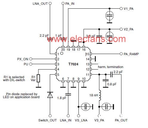
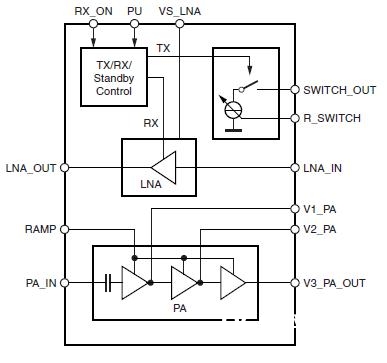
T7024功用框图/T7024 Block Diagram
T7024蓝牙芯片管脚引脚界说:
Table 2-1. Pin DescripTIon
Pin Symbol FuncTIon
1 LNA_OUT Low-noise amplifier output
2 RX_ON RX acTIve high
3 PU Power-up acTIve high
4 R_SWITCH Resistor to GND sets the PIN diode current
5 SWITCH_OUT Switched current output for PIN diode
6 GND Ground
7 LNA_IN Low-noise amplifier input
8 GND Ground
9 VS_LNA Supply voltage input for low-noise amplifier
10 GND Ground
11 V3_PA_OUT Inductor to power supply and matching network for power amplifier output
12 V3_PA_OUT Inductor to power supply and matching network for power amplifier output
13 V3_PA_OUT Inductor to power supply and matching network for power amplifier output
14 GND Ground
15 RAMP Power ramping control input
16 V2_PA Inductor to power supply for power amplifier
17 V2_PA Inductor to power supply for power amplifier
18 GND Ground
19 V1_PA Supply voltage for power amplifier
20 PA_IN Power amplifier input
Slug GND Ground
T7024蓝牙芯片材料介绍
The T7024 is a monolithic SiGe transmit/receive front-end IC with power amplifier,
low-noise amplifier and T/R switch driver. It is especially designed for operation in
TDMA systems like Bluetooth and WDCT.
Due to the ramp-control feature and a very low quiescent current, an external switch
transistor for VS is not required.