ADI公司的ADMV1014是选用硅锗(SiGe)规划的宽带微波下变频器,针对点到点微波无线电规划进行优化,作业频率规模为 24.5-43.5 GHz.它供给两种频率转化形式.能够从正交解调直接变频为基带IQ 输出信号,并从镜像按捺下变频为复中频输出载波频率.基带输出可选用直流耦合,或更典型的是,IQ 输出将使用足够低的高通转机频率进行沟通耦合,以保证足够的解调精度.SPI 接口可对正交相位进行微调,使用户能够优化 IQ 解调功用.高度集成的ADMV1013微波上变频器和ADMV1014微波下变频器十分适用于作业在28 GHz和39 GHz 5G无线基础设施频带下的微波无线电渠道.这些转化器具有1GHz带宽,以及OIP3高于20 dBm的上变频器,能够支撑苛刻的调制计划(如1024QAM),可支撑多Gb无线数据.此外,该芯片组也支撑其他使用如卫星和地上接收站宽带通讯链路,航空无线电,RF测验设备和雷达体系.其杰出的线性度和镜像按捺功用特别合适提高微波收发器规模.本文介绍了ADMV1014首要特性,功用框图以及评价板ADMV1014-EVALZ首要特性,配置图,实验室I/Q形式和IF形式配置图,电路图,资料清单和PCB规划图.
The ADMV1014 is a silicon germanium (SiGe), wideband, microwave downconverter optimized for point to point microwave radio designs operaTIng in the 24 GHz to 44 GHz frequency range.
The downconverter offers two modes of frequency translaTIon. The device is capable of direct quadrature demodulaTIon to baseband inphase (I)/quadrature (Q) output signals, as well as image rejecTIon downconversion to a complex intermediate frequency (IF) output carrier frequency. The baseband outputs can be dc-coupled, or, more typically, the I/Q outputs are ac-coupled with a sufficiently low high-pass corner frequency to ensure adequate demodulation accuracy. The serial port interface (SPI) allows fine adjustment of the quadrature phase to allow the user to optimize I/Q demodulation performance. Alternatively, the baseband I/Q outputs can be disabled, and the I/Q signals can be passed through an on-chip active balun to provide two single-ended complex IF outputs anywhere between 800 MHz and 6000 MHz. When used as an image rejecting downconverter, the unwanted image term is typically suppressed to better than 30 dBc below the wanted sideband. The ADMV1014 offers a flexible local oscillator (LO) system, including a frequency quadruple option allowing up to a 41 GHz range of LO input frequencies to cover a radio frequency (RF) input range as wide as 24 GHz to 44 GHz. A square law power detector is provided to allow monitoring of the power levels at the mixer inputs. The detector output provides closed-loop control of the RF input variable attenuator through an external op amp error integrator circuit option.
The ADMV1014 downconverter comes in a compact, thermally enhanced, 5 mm × 5 mm LGA package. The ADMV1014 operates over the −40℃ to +85℃ case temperature range.
ADMV1014首要特性:
Wideband RF input frequency range: 24 GHz to 44 GHz
2 downconversion modes
Direct conversion from RF to baseband I/Q
Image rejecting downconversion to complex IF
LO input frequency range: 5.4 GHz to 10.25 GHz
LO quadrupler for up to 41 GHz
Matched 50 Ω, single-ended RF input, and complex IF outputs
Option between matched 100 Ω balanced or 50 Ω single-ended LO inputs
100 Ω balanced baseband I/Q output impedance with adjustable output common-mode voltage level
Image rejection optimization
Square law power detector for setting mixer input power
Variable attenuator for receiver power control
Programmable via a 4-wire SPI interface
32-terminal, 5 mm×5 mm LGA package
ADMV1014使用:
Point to point microwave radios
Radar, electronic warfare systems
Instrumentation, automatic test equipment(ATE)
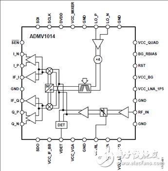
图1.ADMV1014功用框图
评价板ADMV1014-EVALZ
Evaluating the ADMV1014 24.5 GHz to 43.5 GHz, Wideband Downconverter
The ADMV1014 is a silicon germanium (SiGe) design, wideband, microwave downconverter optimized for point to point microwave radio designs operating in the 24.5 GHz to 43.5 GHz frequency range.
The downconverter offers two modes of frequency translation. The device is capable of direct quadrature demodulation to baseband I/Q output signals, as well as image rejection downconversion to a complex intermediate frequency (IF) output carrier frequency. The baseband outputs can be dc-coupled. More typically, the I/Q outputs are ac-coupled with a sufficiently low high-pass corner frequency to ensure adequate demodulation accuracy. The serial port interface (SPI) allows fine adjustment of the quadrature phase to allow the user to optimize I/Q demodulation performance. Alternatively, the baseband I/Q outputs can be disabled, and the I/Q signals can be passed through an on-chip active balun to provide two single-ended, quadrature, complex IF outputs between 800 MHz and 6000 MHz. When used as an image rejecting downconverter, the unwanted image term is typically suppressed to better than 30 dBc below the desired sideband.
The ADMV1014 offers a flexible local oscillator (LO) system, including a frequency quadruple option allowing a range of LO frequencies from 21.6 GHz to 41 GHz to cover a radio frequency (RF) input range as wide as 24.5 GHz to 44 GHz. A square law power detector is provided to allow monitoring of the power levels at the mixer inputs. The detector output can be used to provide closed-loop control of the RF input variable attenuator through an external op-amp error integrator circuit.
The ADMV1014 downconverter comes in a compact, thermally enhanced, 5 mm × 5 mm flip chip CSP package. The ADMV1014 operates over the −40°C to +85°C case temperature range.
The ADMV1014-EVALZ evaluation board incorporates the ADMV1014 with a microcontroller, low dropout (LDO) regulators, and nanoDAC® to allow quick and easy evaluation of the ADMV1014. The microcontroller allows the user to configure the ADMV1014 register map through the ACE software. The LDO regulators allow the ADMV1014 to be powered on by a single supply and offer good power supply ripple rejection. The nanoDAC allows the user to attenuate the RF power going into the mixer of ADMV1014 without using an external power supply.
For full details on the ADMV1014, see the ADMV1014 data sheet, which must be consulted in conjunction with this ADMV1014-EVALZ evaluation board user guide when using this evaluation board.
评价板ADMV1014-EVA首要特性:
Full featured evaluation board for the ADMV1014
On-board USB for SPI control
5 V operation
ACE software interface for SPI control
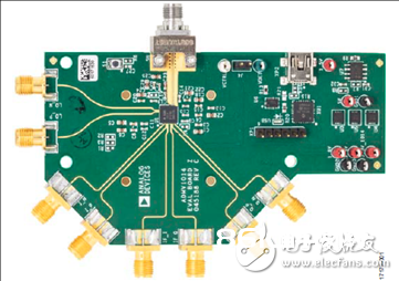
图2.评价板ADMV1014-EVALZ外形图
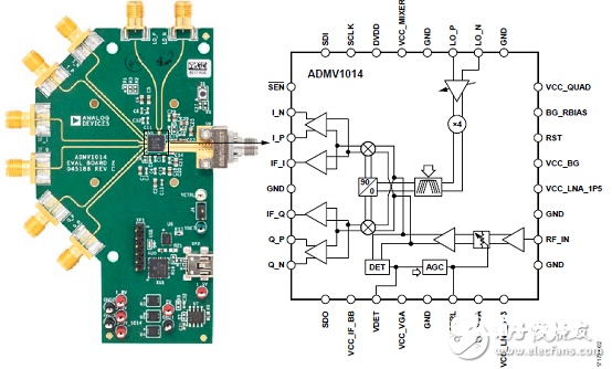
图3.评价板ADMV1014-EVALZ配置图
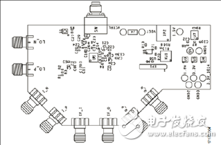
图4.评价板ADMV1014-EVALZ顶视图

图5.评价板ADMV1014-EVALZ实验室I/Q形式配置图
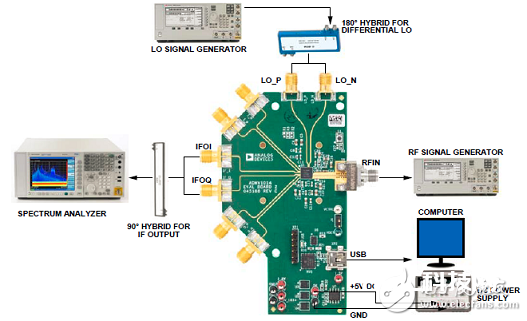
图6.评价板ADMV1014-EVALZ实验室IF形式配置图
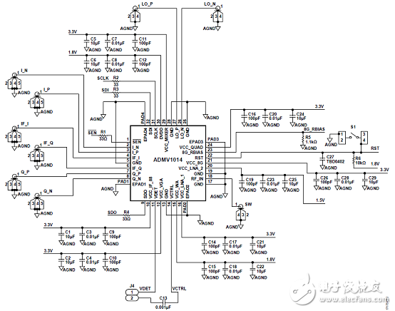
图7.评价板ADMV1014-EVALZ电路图:ADMV1014衔接
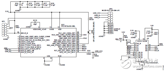
图8.评价板ADMV1014-EVALZ电路图:MCU和电平搬运衔接
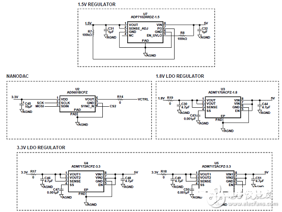
图9.评价板ADMV1014-EVALZ电路图:LDO稳压器衔接
评价板ADMV1014-EVALZ资料清单:
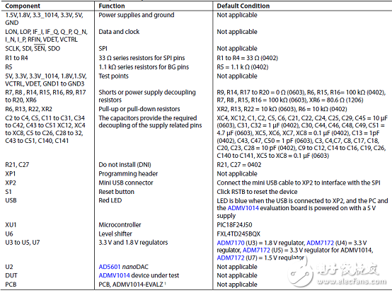
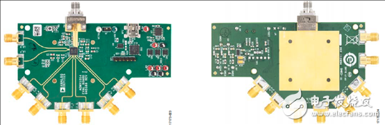
图10.评价板ADMV1014-EVA规划图:左:顶层;右:底层
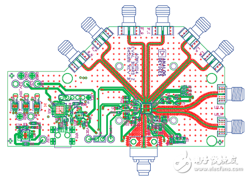
图11.评价板ADMV1014-EVA PCB规划图:顶层
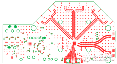
图12.评价板ADMV1014-EVA PCB规划图:第二层电压
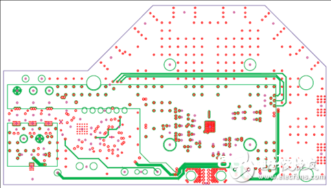
图13.评价板ADMV1014-EVA PCB规划图:第三层
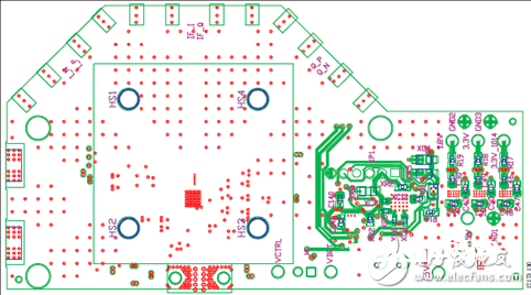
图14.评价板ADMV1014-EVA PCB规划图:底层