文章转自ADI官网,版权归属原作者一切
[Ed. When Dr. Leif was about thirty, well before the turn of the century, he joined Analog Devices as an IC designer. He came with ample prior experience—both for this work and for his age. This wealth of experience included abundant knowledge about measurement instruments and control systems, traceable to his teenage years making radio receivers, transmitters, and TV sets, using surplus components purchased through telak companies (today’s term, from “tele-acquisition,” used during the first decade of the century).
Dr. Leif has spent about as much of his time in teaching analog circuit principles as in direct design. Earlier, he wrote numerous “memos”—brief monographs—which were at one time widely consulted by his fellow designers and avidly read by newcomers to the company. Many of these were later transferred to e-form. Regrettably, these versions were lost during the period known as the “Information Age,” as the “written word” was entrusted to progressively obsolescent generations of storage modalities and media. It was a time when everyone was suffocating under a glut of “data” while experiencing a dearth of deep-seated knowledge about analog design: “The Fundaments,” as Newton Leif likes to call the essential principles, the roots of physical phenomena.
Recently, when a young engineer named Niku Chen joined his team at our Design Center in Solna, he encouraged her interest in recovering whatever of this treasure trove she could. Here is one such article that she found, written in 2008, reproduced in facsimile form. We trust it contains few, if any, errors. His prose, written in the American English of first-decade 21st century, is more flowery than we expect in 2029. The header indicates that Leif (who is still with ADI in Solna, and active in the field) was evidently very familiar with the Fundaments of Noise back then. But he also wanders around quite a bit in this odd little piece. These editorial comments are occasionally interpolated.]
Leif 2698:060508 Noise in Logarithmic Amplifiers
We occasionally receive inquiries about the noise figure of log amps. Whether this is a valuable metric in their common use as power measurement elements is for the user to decide. However, whenever a log-limiting amplifier is used in the signal path (in PM or FM applications), noise figure is clearly important, since it provides a measure of that system’s ability to extract information from a signal in the presence of noise. Accordingly, this metric should be provided, in the event it is required for inclusion into a user’s spreadsheet estimation of a system’s performance. This memo is for field application engineers and customers alike.
Monolithic, fully calibrated logarithmic amplifiers (log amps), pioneered by Analog Devices over the past twenty years, are uniquely equipped as RF measurement elements at frequencies from near-dc up to 12 GHz in the latest products. Their special value stems in part from having a wide “dynamic range” and in part from presenting their measured values directly as decibel quantities. They are temperature-stable and exhibit excellent conformance to a “log law.” The focus of this memo is on some limitations imposed by basic noise mechanisms. As always, in digging down to root causes, some side trips will be needed.
Log amps come in three basic forms. However, in their capacity as RF power-measurement devices, we are mainly concerned here with the first two types:
- Those employing multistage amplification and progressive limiting1 generate a close approximation to the logarithm in a piecewise fashion. Some of these parts also make available the output of the final limiting-amplifier stage, for extracting time-encoded information (PM or FM, baseband bit streams). These include the AD608, AD640/AD641 and the extensive AD8306, AD8307, AD8309, AD8310, AD8311, AD8312, AD8313, AD8314, AD8315, AD8316, AD8317, AD8318, and AD8319 family, as well as closely matched dual log amps, such as the AD8302 (which also measures phase), and the ADL5519, having an unprecedented 1 kHz to 10 GHz measurement range.†
These progressive-compression log amps include a rectifier (detector) with each of five to 10 low-gain (8 dB to 12 dB) stages, whose outputs are summed to produce a filtered voltage that is a decibel-scaled measure of average power. Where the final hard-limited signal is also provided (as in the 100-dB range products AD8306/AD8309), the logarithmic measure is often viewed as ancillary, and referred to as the received-signal-strength indicator (RSSI).
- Those using an exponential-gain amplifier (X-AMP®architecture)2 with a 60-dB typical gain span, followed by a single detector whose filtered output is compared to a reference level; the integrated error generates a voltage, which adjusts the amplifier gain to null the error (see text associated with Figure 6). That voltage is a representation of the decibel value of the applied signal, due to the accurate exponential (sometimes called “linear-in-dB”) gain function. By giving the detector a square-law response, it is the power-equivalent (rms) value of the applied signal that is measured.
This will be recognized as the general form of an automatic-gain-control (AGC) amplifier. Accordingly, we can call them AGC-style log amps. The AD8362, AD8363, and AD8364 are of this type, the latter two providing the simultaneous measurement and differencing of two input signals. In this type, there is usually no provision to access the amplified signal. An exception is the AD607 (actually a single-chip superheterodyne receiver), whose decibel-scaled RSSI output spans 100 dB, and whose signal outputs are the I/Q components of the demodulated IF.
- Those based on the uncannily reliable translinear properties of a bipolar junction transistor (BJT)—the precise logarithmic relationship between its base-emitter voltage (VBE) and its collector current (IC) over a range of up to 10 decades of current (200 dB!). An early exploitation of this property in conjunction with an op amp was due to Paterson.3
Modern products, now known as translinear log amps, are similar, deviating only in the details of implementation. This separate class of log amps, used in fiber-optic communication systems to measure optical power and control the gain of optical-mode amplifiers, only measures essentially static currents, from as low as 1 picoamp up to several milliamps. Alternatively, using external input resistors, voltages with a large range of amplitudes can also be measured. Examples include the AD8304, AD8305, ADL5306, and ADL5310.
Background
Any system’s internal noise is a result of the fundamental thermal energy, kT, thus its absolute operating temperature, T (where k is Boltzmann’s constant). In one case of general interest, the root source is an antenna, whose noise results from the electromagnetic coupling into the free-space resistance from which it receives its signal, and which has the basic value of 377 ohms. The signal and noise are equally coupled into the system via a first impedance transformation created by the design of the antenna, and thence conveyed by a cable of the same impedance. They operate at their greatest power efficiency in driving, say, a 300-ohm balanced (“twin” or “ribbon”) feeder, or alternatively a 50-ohm (or occasionally a 75-ohm) coaxial cable.
As an aside, the minimum loss in a coaxial cable occurs when its characteristic impedance is 71 ohms. Above this, the resistance of the thinning inner conductor increases the loss; below, it is the thinning dielectric layer that increases loss. While not optimal, 50 ohms has become the resistance reference level for measurement, largely for reasons of convenience and standardization. Unless otherwise stated, it is the value used in specifying noise figure.
As a power source (really, a transducer, from electromagnetic to electrical power) an antenna exhibits a complex impedance ZA = Re(ZA) + jIm(ZA). Nevertheless, it acts purely resistive over a generally narrow range of frequencies. Clearly, the power it can deliver to an open-circuit—such as an ideal voltage-responding element—is zero, since none of the available current is extracted from the source. Similarly, the power into a short circuit—such as an ideal current-responding element—is zero, since none of the voltage swing is used. The power-transfer theorem shows that the maximum power that can be delivered to a load connected to this source occurs when the resistive part of the load impedance is made equal to RA = Re(ZA), say, 50 ohms (Figure 1).

Log amps intended for RF power measurement (often referred to simply as RF detectors) do not generally require extremely low noise figures. Instead, the design emphasis in the first amplifier stage is to minimize the voltage-noise spectral density (VNSD), typically a few nV/√Hz, and its noise performance is specified in this way. When this VNSD is integrated over the log-amp’s RF bandwidth (not the post-detection—or so-called video—bandwidth), the rms noise typically amounts to tens of microvolts. only when this voltage is referred to the impedance level at the input can the device’s internal noise be expressed as a power level (as so many dBm: decibels relative to 1 mW). The integrated noise voltage sets a bound on the smallest input voltage that can be measured with certainty—and thus indirectly on the minimum signal power.
Figure 2 shows how this lower bound on the dynamic range can be expressed as power for various choices of impedance. Note that the response, illustrated for a typical scaling of 20 mV/dB (400 mV/decade), is specifically for a sine wave input; a 0-dBV input signifies a sine input whose rms amplitude is 1 V. Below each axis marker is the corresponding power level when the voltage is applied to a termination resistor of 50 ohms or 316 ohms.

In an earlier monograph, LEIF 2131:080488*, I discuss how the basic RF log-amp types compare in responding to various other waveforms. For many years the effect of the signal’s waveform on the logarithmic intercept (often misleadingly called “offset”) went largely unnoticed because early log amps were fairly crude and needed to be manually adjusted in situ. As the first complete, fully calibrated multistage log amp, the AD640 changed all that. Elsewhere4 I have shown that log amp design need no longer be empirical (as it certainly used to be5).
*[Ed. We may be able to acquire this document (if Niku Chen found it) and publish it in Analog Dialogue at a later date].
Johnson-Nyquist Noise
An ideal matched-input antenna amplifier absorbs the maximum available power, while adding no noise of its own. But—apart from naturally occurring noise sources in the surroundings—the antenna will have its own noise, typically referred to the 50-ohm impedance level, just as any resistor generates noise. Note that this is not the consequence of some particular manufacturing technology, although there are additional noise mechanisms at work, to varying degrees, in most practical resistors.
Resistor noise was first noted by Johnson6 and later analyzed and quantified by Nyquist.7 It is the electrical manifestation of the random motion of current carriers in a conductive medium. Nyquist observed that the energy of this motion can be stated in terms of the Boltzmann constant, k, and absolute temperature, T, which translates to noise power, PN (that is, energy/unit-time). It is customary to express time in reciprocal form, as the system bandwidth, B (hertz). The result is as simple as it is fundamental: the noise power associated with a conductor is just kTB (watts).
Now consider a real resistor, R, at an absolute temperature, T, connected to an ideal noise-free resistance, RO, of equal value. Here, the noise voltage, EN, of the resistor, R, is halved by virtue of the load, RO, the latter generating no noise. So the noise power in R is simply (EN/2)2/R, which must be equal to the kTB noise power; that is, EN2/(4R) = kTB. Thus, EN = √4kTRB V rms.
Noise-figure specifications assume (somewhat arbitrarily) that an antenna “operates at” a temperature of 290 K (16.85°C). What is really being referred to here is not the actual temperature of the metal elements comprising the antenna, nor the air temperature that surrounds it; even less the temperature of the directionally narrow source of the signal. Rather, it is the average temperature of all the material objects within the full scope of the antenna’s “view,” modified by its polar diagram (sensitivity vs. direction). The background temperature (thus kT), near Stockholm during winter, as perceived by an antenna seeking a source beyond the warm buildings, may actually be much higher than in pointing the antenna to the Nevada sky (though, in fact, air temperature will have a small effect on the antenna’s intrinsic noise figure).
At 290 K the open-circuit VNSD of a 50-ohm antenna, like that of any other resistor, is 894.85 pV/√Hz. Applied to a noise-free load of 50 ohms, the noise voltage at the load is halved, to 447.43 pV/√Hz, so the noise power is this voltage squared divided by 50 ohms, or 4 × 10–21 W/Hz (note: no longer √Hz). Expressed as a power spectral density in milliwatts, this is –173.975 dBm/Hz. Not surprisingly, it is called the thermal noise floor.
Notice that the impedance level is arbitrary; the noise floor would still be –174 dBm/Hz if the antenna were matched into a 75-ohm load. This is evident when we note that, in the above calculation, the quantity √4kTR was first halved to get √kTR as the load voltage, which was then squared, giving kTR, and then divided by the same resistance (assuming matching), coming back to kT.
[Ed. This is rock bottom. But, of course, the temperatures of the active devices that follow the antenna can be lowered. In today’s cosmotronics, a zygomaser (those dual-path masers, operating at cryogenic temperatures) is used as the low-noise amplifier. But a pair of such masers isn’t cheap, and they won’t fit too well into the typical wrist-worn HSIO Municator!]
Noise Figure and Noise Mechanisms
If the first-stage amplifier is not ideal, it will add its own noise to the signal. So let’s suppose that an exceptionally quiet op amp is used as a voltage-mode amplifier. To ensure that the source—for example, an antenna—is properly terminated, a 50-ohm resistor is placed across the signal-input port of this amplifier. Before even considering the op amp’s own internal noise, we’ve degraded the noise figure by 3 dB. Here’s why. First, the definitions:

As we’ve seen, the open-circuited signal voltage, VIN, is associated with an open-circuit noise voltage, say EN—the voltage noise spectral density (VNSD)—integrated over the system bandwidth. Again, imagining a load formed by a noise-free impedance of 50 ohms, the signal voltage across this load is halved, to VIN/2, while its noise voltage is also halved, to EN/2. Thus, the signal-to-noise voltage ratio and, consequently, the signal-to-noise power ratio, remain unaffected. The noise factor is unity, and the noise figure (hereafter NF) is 0 dB.
Of course, this is only possible using a noise-free load. Such ideality is conceivable when the load is created from reactances. For example, √L/C has the dimensions of resistance, while an L/C network, in principle, has no loss. Even real L/C networks, have very low loss: they are essentially nondissipative. (By contrast, resistors convert power into heat, which is then lost to the universe.) But even when assisted by the magic of L’s and C’s, the elements essential to providing power gain, the active devices inherently have ohmic resistance to degrade the NF.
Shot Noise
Junction devices also exhibit fundamental shot-noise phenomena, emerging from a different sort of stochastic mechanism, namely, the granularity of an electric current crossing a potential barrier. This was first observed by Schottky8 in the electrons emitted from the cathode of a vacuum diode. Being released randomly, they form a Poisson sequence of events—each electron, like a honeybee, faithfully carrying its precise little packet of charge, q = 1.602 × 10⁻¹⁹ coulombs.
A similar process arises in injecting carriers from the emitter into the base of a BJT. Fluctuations in emission/injection are due to the continual tiny changes in the carrier energy against the work-function of a cathode, or the band-gap energy of a semiconductor junction. In the latter case (unlike a vacuum diode), some of the injected carriers recombine in the base region(s), where there are other smaller noise mechanisms; and the noise at the collector is modified accordingly. Thus, it is known as collector shot noise—but confusingly, since the root cause is at the initial injection site.
You should note that Johnson noise is due to the random motion of carriers in a conductive medium, while shot noise is due to the random occurrence of these carriers as they encounter a barrier.
It is readily shown that the magnitude of the spectral density of the shot noise current, in A/√Hz, is √2qI, where q is the electron charge and I is the mean bias current, taken as IC for a transistor. For example, at a collector current of 1 mA, this noise amounts to 17.9 pA/√Hz. However, unlike the resistor’s noise, shot noise is temperature-independent (when all the detailed local mechanisms, including the temperature-dependence of transconductance, are combined for the case of the transistor). It is no more than a manifestation of the granularity of a current. Further, while resistor noise directly represents power, shot noise is only a fluctuation in current and thus corresponds to some power only when it flows in an impedance, often at some “output.”
Now, such an impedance (not the “collector output resistance”) exists within a transistor. It is the “incremental emitter resistance,” re, the inverse of the small-signal transconductance, equal to kT/qIC. This gives rise to a noise voltage, which can be referred to the base-emitter port; it has a spectral density that is the product of the noise current and this resistance, amounting to kT/qIC × √2qIC, which reduces to kT√2/qIC.
At IC = 1 mA and 27°C, this amounts to VNSD of 463 pV/√Hz (Figure 3). Keep in mind that re is not an ohmic resistance, but simply the partial derivative, ∂VBE/∂IC, and thus it is noise-free (which is why it is shown using a distinctive symbol). However, it is interesting to note that the said product of the shot noise current and this resistance is identical to the noise voltage generated by a real resistance of half its value. Here, for example, re is 25.86 ohms, and the noise of a real 12.93-ohm resistor is also 463 pV/√Hz. This is simply because the “shot-noise-times-re” can be written as 2√(kT)2/qI = √2kTre which is √4kT(re/2). This quantity equates to √4kTR, the Johnson noise of a resistor, R, only when R = re/2. This must clearly “work out right.” It does leave some perplexing questions, though. Why is there such an amusing convergence of these two apparently very disparate fundamental noise processes? That’s a topic for another (long) memo!

Aspects of Low-Noise Amplifier Design
The design of matched-impedance low-noise amplifiers is a large topic in its own right; but it is useful to consider how some basic aspects of the BJT (of any modern technology, noting that SiGe and other exotic heterojunction transistors are just BJTs on steroids) set a fundamental lower bound on the noise figure, even before the effects of the unavoidable contacting resistors, RBB’ and REE’, are included in the recipe.
Figure 4 shows what at first appears to be a highly rudimentary and incomplete circuit, little more than a diode-connected transistor with a resistor, RF, in its base, and biased by a current source. Surprisingly, this is a practical (although not optimal) low-noise amplifier (LNA): its VCE, the sum of the VBE and the voltage drop across RF, is quite sufficient for these illustrative purposes; and there are numerous ways to elaborate this basic form while retaining the relevance of this analysis.

The approach may be called the translinear viewpoint of LNAs, since it starts with an ideal resistance-free transistor model (see “Foundation Design,” Leif 1677:011284)* and demonstrates how one can gain profound insights into behavior that turns out to be both beautiful in certain respects, yet deeply complex in others.
*[Ed. There follows in the Leif monograph a rather philosophical account of how the value of the feedback resistor, RF, can be seen as necessarily having to equal RA2/re if a reciprocal match to the source and load is required, without recourse to mathematics. His basic point is that there are only three key resistances in the circuit: The unknown, RF, and the knowns, RA and the BJT’s re. So (according to Leif) there are only two dimensionally correct ways of linking them: either RF = re2/RA or RF = RA2/re. The first of these is clearly incorrect.]
Now, the strange thing about this little circuit is that the match is precisely preserved for every value of IC from zero on up! This assumes that we arrange for RF to track re in the manner shown, which means giving it the algorithmic value qICRA2/kT. It follows, as is so often the case, that IC must be proportional to absolute temperature (PTAT) to maintain this match—and a temperature-stable gain having the signed value 1 – qICRA/kT.
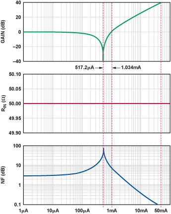
This can be seen by setting IC = 0, when RF is obliged to also be zero. Then the transistor has no transconductance, and the zero-valued resistance, RF, simply connects the source to the load for a gain of ×1 (that is, 0 dB). At a critical value of current, IC = kT/qRA, that is, 517.2 μA = 25.86 mV/50 ohms, when RA = 50 ohms, the gain becomes zero (i.e., –∞ dB), after which it rises, crossing –1 (back to 0 dB again!) at an IC of precisely 1.034 mA (for T = 300 K).
From that value onward, the gain increases. All the while, the input impedance remains firmly stuck at the value RA, here 50 ohms. Figure 5 shows the input impedance, voltage gain (which is also the power gain when reciprocally-matched), and noise figure. In this ideal simulation, the NF is under 0.4 dB at an IC of 10 mA at which point the gain is ×18.33 (inverting), that is, 25.3 dB.
This analysis is at once optimistic and pessimistic. It is optimistic in neglecting the noise contributions of the transistor resistances, notably RBB’ and REE’, and the consequence of finite small-signal current gain, βAC, which creates a noise current, √2qIC/βAC, which flows in the effective source impedance (including RBB). It is very important to keep in mind that βAC at high frequencies is very much lower than at dc. Its magnitude is closely equal to the device’s fT—for a given geometry and bias—divided by the signal frequency, fS (and its phase is +90°). Thus, for an fT of 10 GHz (it is never as high as its peak value) and an fS of 2 GHz, this BJT’s common-emitter current-gain is a pitiful 5!
Thus, in this example, one-fifth of the collector shot noise, that is, 0.2√2qIC = 11.3 pA/√Hz appears in the base when IC = 10 mA. This operates on the total base impedance, thus at the very least the source impedance of 50 ohms (it need not be resistive), generating 566 pV/√Hz of VNSD. This is over twelve times the 46.3 pV/√Hz due to the re-induced shot noise at this current!
But these figures are pessimistic in neglecting all the ingenious things that can be done using reactive elements around the active device; to drastically lower the NF, although invariably at the expense of distortion (commonly expressed in terms of the input-referred two-tone third-harmonic intercept, IIP3, and less usefully in terms of the 1-dB gain-compression point, P1dB).
[Ed. At the top of this page in our copy of Leif’s monograph, this penciled note appears: “Niku: Here’s a curious aside: using a grounded-base topology with IC = 517 µA to set RIN to 50 ohms, and thus match a 50-ohm source, you will find by spectral analysis that the P1dB point is never reached. The gain error just grazes –0.9 dB at a certain input level, then asymptotically returns to 0 dB. Isn’t that interesting?! Can you figure out what’s going on here?” No date is appended.]
Nonetheless, an NF as low as 0.3 dB is practicable in a high-gain transistor amplifier at room temperature when other attributes (such as linearity) can be relaxed. For example, the amplifier in Figure 1(c) exhibits a noise factor of √(2 + AV)/(1 + AV) using an amplifier with negligible voltage- and current-noise. If we set the gain, AV, to 20 V/V (26 dB), the NF can be as low as 0.2 dB, that is, 20 log10 √22/21 (the first factor is 20 here because we are in the voltage domain), even though the noise due to the feedback resistor is as high as 4.18 nV/Hz when chosen to match a 50-ohm source, that is, to 1.05 kohms. Of course, in practice (darn it!) the amplifier’s input noise will not be negligible.
Power Calibration of a Logarithmic Detector
Very few electronic elements respond directly to power. To do so, they must not only absorb some source power, accurately and completely, as does a resistor; but the heat that is generated in this way must then be measured with corresponding accuracy. When a resistor was included across the input terminals of our ideal voltage-mode amplifier, the power supplied by the source heated up the resistor by a minuscule amount. Just as an example, if the signal power were –30 dBm—that is, one microwatt—and the thermal resistance of the load were, say, 100°C/W, it would heat up by only 100 microdegrees.
This is a tiny temperature change; but some power detectors are nevertheless based directly on measuring the temperature of a low-mass resistor, suspended on ultrathin fibers in such a way as to have an extremely high thermal resistance—perhaps as much as 100,000°C/W. Even then, the temperature changes are only of the order of millidegrees. These truly fundamental power-responding elements are still used at high microwave frequencies, but since the turn of the century, high-accuracy inexpensive IC detectors have been available; they can be used with ease from dc to over 12 GHz.
Some TruPwr™ detectors of the AD8361 and ADL5500/ADL5501 class use analog-computing techniques to magnitude-square the instantaneous waveform values of a signal, thus producing an intermediate output VSQ = kVSIG2. This crucial first step is then followed by averaging and a square-root operation—finally yielding the root-mean-square (rms) value. In designing these products, vigilant attention has to be paid to maintaining low-frequency accuracy at every step, while using circuit techniques that are at the same time accurate with microwave waveforms.
Many of the newer rms-measuring products produced by Analog Devices, also in the TruPwr category, use a high-precision AGC technique (Figure 6). They first amplify the signal from an input level which may be only a few millivolts, then apply this signal to one squaring-cell. Its output is compared to that of an identical cell operating with a fixed input (the “target” voltage: VT). The integrated imbalance in these outputs then either raises or lowers the gain as necessary to restore exact balance between the squarer outputs. Since the variable-gain amplifier used employs X-AMP® architecture, it inherently provides an accurate inverse-exponential gain in response to a control voltage, which thus represents the rms amplitude at the input as a precisely scaled decibel quantity.

An earlier type of power detector, now universally known as a “logarithmic amplifier” (although it usually performs only the measurement function, providing an output proportional to the logarithmic magnitude of the input’s mean voltage amplitude), uses cascaded gain stages of the hard-limiting kind. It is readily demonstrated that the log function arises naturally as a piecewise approximation when the output of each cell contributes to a progressively increasing sum.4 Note that this operation does not inherently address the need to respond to the “mean-square” or “true power” of the input—although, as a matter of interest, the response to noise-like signals does in fact closely track their rms value. Figure 7 shows an illustrative schematic of this type, the progressive-compression log amp.

Noise Figure and Logarithmic Detectors
It will by now be very clear that none of these detectors respond to the power of a signal being absorbed at their input. Rather, the response is strictly to the voltage waveform of the signal. All of the signal’s power is absorbed by the resistive component of the input impedance, which is in part internal to the IC, and in part added externally to lower this impedance, commonly down to 50 ohms. This casts doubt on the value of an NF specification. Ideally, the sensitivity and measurement range of log amps of these types ought never to be specified in “dBm”—which refers to power in decibels above 1 mW—but always in “dBV,” the decibel level of a voltage relative to 1 V rms. A signal of this amplitude dissipates 20 mW in a 50-ohm resistive load, which amounts to 13.01 dBm re 50 ohms (“referred to a 50-ohm load”).
Nevertheless, provided the net shunt resistance at the log amp input is known, graphs of its amplitude response may use a common horizontal axis scaled in both dBm and dBV, offset by a fixed amount, which for 50 ohms is 13 dB, as illustrated in Figure 2. Unfortunately, the RF community does not generally think in dBV terms, and this practice is not rigorously followed. In many data sheets only a dBm scale is used, leading to the appearance of a genuine power response, which, as has been strenuously noted, is never the case for an RF power sensor.
Even when a log amp’s input stage is designed to match the source impedance—which makes better use of all the available power and usefully lowers the noise floor—the response is still to the voltage appearing at the input port. Of course, this does not mar its utility as a power-measuring device. At lower frequencies it is easy to design ICs that explicitly sample both the voltage and current in and through a load. An example of this practice is found in the ADM1191.
Recall that, for the case of a 50-ohm source, loaded by a 50-ohm resistor, the degradation in noise figure, to 3 dB, was entirely due to the additional noise of the termination resistor. When the measurement device presents an open circuit to the source either the input is shunted with a 50-ohm resistor to set the effective power-response scale; or the input is padded down to 50 ohms from the log amp’s finite RIN. The noise voltage associated with the input port is no longer simply the Johnson noise of this resistance; it is now the vector-sum of that noise voltage and the input noise voltage of the measurement device. Furthermore, the log amp’s inherent input noise current will be multiplied by this net shunt resistance, and the resulting voltage, if significant, may need to be included in the vector sum. However, it is usually already included, indirectly, in the input-referred VNSD specification.
Suppose the latter is stated as 1 nV/√Hz. Next, take the 300 K (27°C) value—the typical operating temperature of a PC board—for the Johnson noise at 25 ohms (the 50-ohm source in shunt with the net 50 ohms of the external loading resistor and the log amp’s RIN) as √4kTR = √4k × 300 × 25 = 643.6 pV/√Hz. Now, the vector-sum of these is 1.19 nV/√Hz. Arbitrarily assigning a unit amplitude to the “signal,” (noting that the 300 K noise for the 50-ohm source is 910 pV/√Hz) we have:

The more general form for the case of a 50-ohm source and 50-ohm load is 20 log10(2.2 × 10⁹ √0.64362+ VNSD2). Below is a short table of noise figure (NF) for several values of the voltage noise spectral density at the log amp’s input, assuming a 50-ohm source and a net resistive load at the log amp’s input of 50 ohms.
| VNSD (nV/√Hz) | NF (dB) |
| 0.00 | 3.012 |
| 0.60 | 5.728 |
| 1.00 | 8.345 |
| 1.20 | 9.521 |
| 1.50 | 11.095 |
| 2.00 | 13.288 |
| 2.50 | 15.077 |
baseline Sensitivity of a Logarithmic Detector
As noted, noise figure is a relevant metric when the log amp being quantified is a multistage limiting amplifier, providing signal output, which may also operate as a detector, providing an RSSI output—for example, the AD8309. This part is specified as having an input-referred noise (VNSD) of 1.28 nV/√Hz when driven from a terminated 50-ohm source (that is, with a net 25 ohms of resistance across its input port). From the expression provided above, this amounts to an NF of 9.963 dB. The data sheet value of NF (p. 1) is 6 dB lower, at 3 dB, based on taking the ratio 1.28 nV to the 50-ohm VNSD of 0.91 nV, with a decibel equivalent of 20 log10(1.28/0.91) = 2.96 dB.
The baseline sensitivity of a log amp is limited by its bandwidth. For example, assume a total VNSD at the input of a log amp (whether the progressive compression or AGC type) of 1.68 nV/√Hz and an effective noise bandwidth of 800 MHz. The integrated RTI noise over this bandwidth is 47.5 μV rms (that is, 1.68 nV/√Hz × √8 × 10⁸ Hz). Expressed in dBm re 50 ohms, this is 10 log10(Noise Power) = 10 log10(47.5 mV2/50 ohms) = –73.46 dBm.
This “measurement floor” is a more useful metric than NF, since it shows that measurements of signal power below this level will be inaccurate. Here, it will be found that the indicated power for an actual single-tone sine wave input near –73.46 dBm floor will be very close to the same value, assuming the noise waveform is Gaussian. As another example, the input-referred noise spectral density of the AD8318 is found (in the first column of Page 11 of the Rev. B data sheet) to be 1.15 nV/√Hz, which amounts to an integrated noise voltage of 118 μV rms in that part’s 10.5-GHz bandwidth. This is a noise power of –66 dBm, re-50 ohms. The user should also be aware that, in a progressive-compression log amp having too few stages, the measurement floor may be determined, not by noise, but simply by insufficient gain.
参阅电路
1www.analog.com/en/analog-dialogue/articles/monolithic-dc-to-120-mhz-log-amp.html
2www.analog.com/en/analog-dialogue/articles/low-noise-wideband-amp-linear-in-db-gain.html
3Paterson, W. L. “Multiplication and Logarithmic Conversion by Operational-Amplifier-Transistor Circuits.” Rev. Sci. Instr. 34-12, Dec. 1963.
4Gilbert, B. “Monolithic Logarithmic Amplifiers.” Lausanne, Switzerland. Mead Education S.A. Course Notes. [1988?]
5Hughes, R. S. Logarithmic Amplification: with Application to Radar and EW. Dedham, MA: Artech, 1986.
6Johnson, J. B. “Thermal Agitation of Electricity in Conductors.” Phys. Rev. 32, 1928, p. 97.
7Nyquist, H. “Thermal Agitation of Electronic Charge in Conductors.” Phys. Rev. 32, 1928, p. 110.
8Van der Ziel, A. Noise. Prentice Hall, 1954.
*[Ed. Note—The two earliest papers in this series, “The Four Dees of Analog, circa 2025″ (1), and “The Fourth Dee: Turning Over a New Leif” (2) were not numbered when originally published.]
†Information and data sheets on all products mentioned here may be found on the Analog Devices website, www.analog.com.