文章转自ADI官网,版权归属原作者一切
Introduction
Applications such as automated test equipment, machine automation, industrial, and medical instrumentation require precision data acquisition systems in order to analyze and digitize physical or analog information accurately. System designers who want to achieve full data sheet specifications from high resolution, precision successive approximation register (SAR) ADCs are often forced to use a dedicated high power, high speed amplifier to drive the traditional switched capacitor SAR ADC inputs for their precision applications. This is one of the common pain points encountered in designing a precision data acquisition signal chain, and this article presents the pin-compatible AD4000 ADC family that addresses this issue. Designed using ADI’s advanced technology and state-of-the art architecture, this family of 16-/18-/20-bit precision SAR ADCs incorporates ease of use features that offer a multitude of system-level benefits that enable reduced signal chain power and complexity, and higher channel density without significantly compromising performance. A unique combination of high-Z mode, reduced input current coupled with long acquisition phase eases the ADC driving challenge and reduces the settling requirement on the ADC driver. This broadens the amplifier choice for driving the ADC to lower power/bandwidth precision amplifiers including JFET and instrumentation amplifiers for dc or low frequency (<10 kHz) applications. This is a follow-up version to a previously published Analog Dialogue1 article that will present a wide range of precision amplifiers with a lower RC filter cutoff that can directly drive this ADC while achieving optimum performance—eliminating a dedicated ADC driver stage and significantly saving system power, board space, and BOM cost.
Driving Traditional SAR ADC Input
Figure 1 shows a typical signal chain used in building precision data acquisition systems. Driving high resolution, precision SAR ADCs has traditionally been one of the major pain points and a tricky issue for system designers because of the switched capacitor inputs.
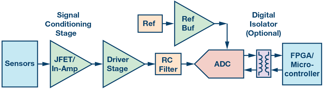
System designers need to pay close attention to the ADC driver data sheet and look at the noise, distortion, input/output voltage headroom/footroom, bandwidth, and settling time specifications. Typically, high speed ADC drivers are required that are wide bandwidth, low noise, and high power in order to settle the switched capacitor kickback of the SAR ADC inputs within the available acquisition time. This significantly reduces the options available for amplifiers to drive the ADC and results in significant performance/power/area trade-offs. Furthermore, selecting an appropriate RC filter to place between the driver and the ADC inputs imposes further constraints on amplifier choice and performance. The RC filter between the ADC driver output and SAR ADC input is required to limit wideband noise and reduce the effects of charge kickback. Typically the system designer needs to spend significant time to evaluate the signal chain to ensure that the selected ADC driver and RC filter can drive the ADC to achieve a desired performance.
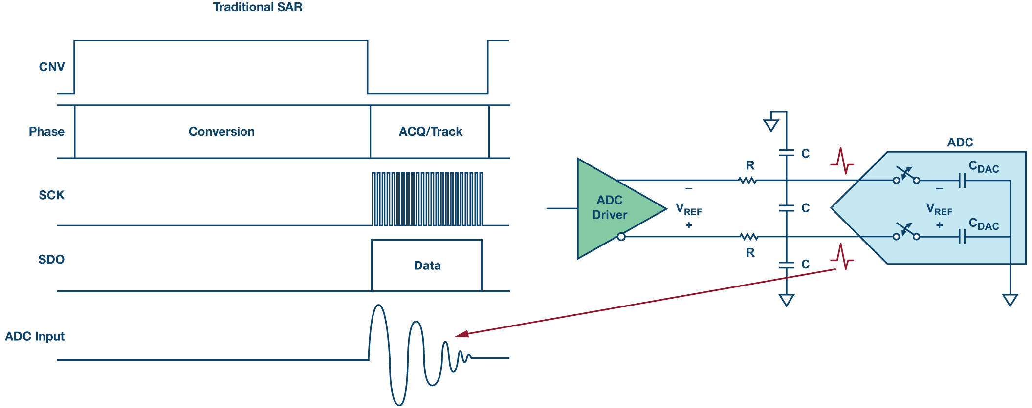
As shown in the Figure 2 timing diagram, SAR ADC throughput (1/cycle time) is comprised of conversion and acquisition phases and the data from the ADC can be clocked out using the serial SPI interface during the acquisition phase. In traditional SAR architecture, the conversion phase is typically longer and the acquisition phase is shorter. During the conversion phase, the ADC capacitor DAC is disconnected from the ADC inputs to perform the SAR conversion. The inputs are reconnected during the acquisition phase, and the ADC driver must settle the nonlinear input kickback to the correct voltage before the next conversion phase begins. The ADC driver cannot settle the traditional SAR ADC kickback within the available acquisition time with aggressive filtering at a lower RC bandwidth cutoff and hence the ADC distortion/linearity performance is degraded.
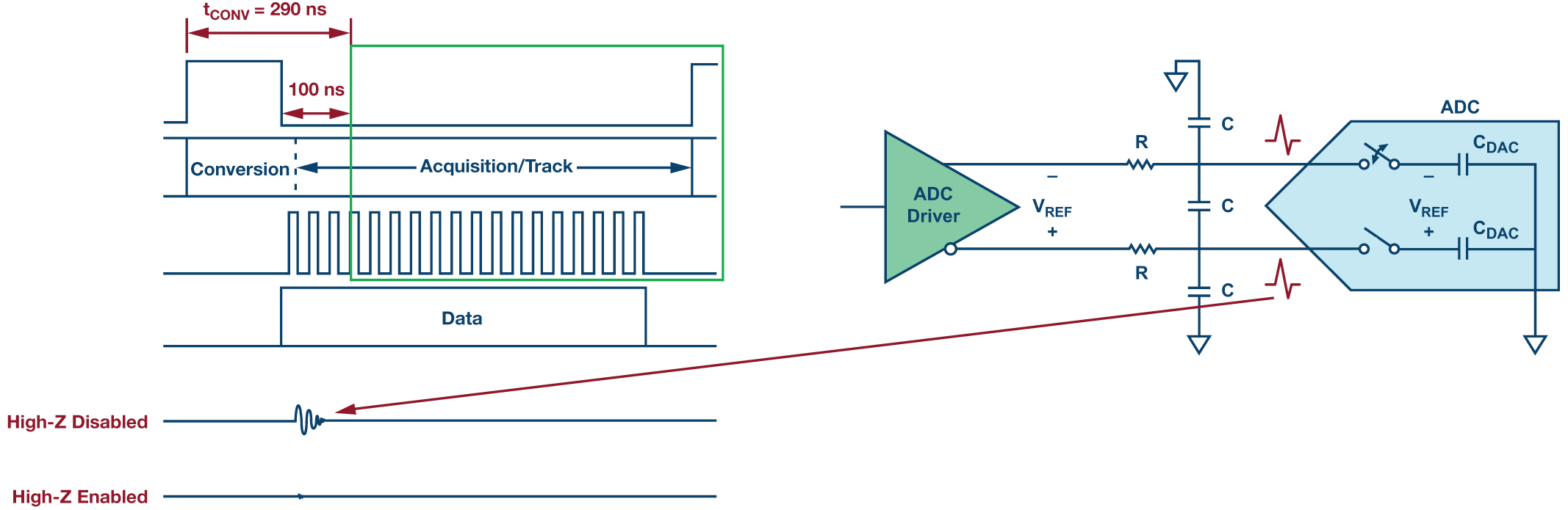
Longer Acquisition Phase
The AD4000 ADC family features a very fast conversion time of 290 ns and the ADC returns back to the acquisition phase 100 ns before the end of the ongoing conversion process, which enables a longer acquisition phase as shown in Figure 3. The nonlinear kickback seen from this ADC family input is significantly reduced even with high-input impedance (Z) mode disabled and it is reduced to almost negligible levels when high-Z mode is enabled. This reduces settling time burden on the ADC driver and it allows a lower RC cutoff with large R, which means a higher noise and/or lower power/bandwidth amplifier can also tolerated. This allows the amplifier and RC filter in front of the ADC to be chosen based on the signal bandwidth of interest and not based on the settling requirements of the switched cap inputs. A larger value of R can be used in the RC filter with a corresponding smaller value of C, which reduces amplifier stability concerns without impacting distortion performance significantly. A larger value of R helps to protect the ADC inputs from overvoltage conditions and it results in reduced dynamic power dissipation in the amplifier. Another benefit of a longer acquisition phase is that it enables a low SPI clock rate to reduce input/output power consumption, broaden the alternatives for processors/FPGAs, and simplify the digital isolation requirements without compromising the ADC throughput.
High-Z Mode
The AD4000 ADC family incorporates a high-Z mode that reduces the nonlinear charge kickback when the capacitor DAC switches back to the input at the start of acquisition. With high-Z mode enabled, the capacitor DAC is charged at the end of conversion to hold the previously sampled voltage. This process reduces any nonlinear charge effects from the conversion process affecting the voltage that is acquired at the ADC input prior to the next sample. The benefits of high-Z mode are the elimination of dedicated high speed ADC drivers and broadening a choice of lower power/bandwidth precision amplifiers, including JFET and instrumentation amplifiers for low frequency (<10 kHz) or dc type signals.
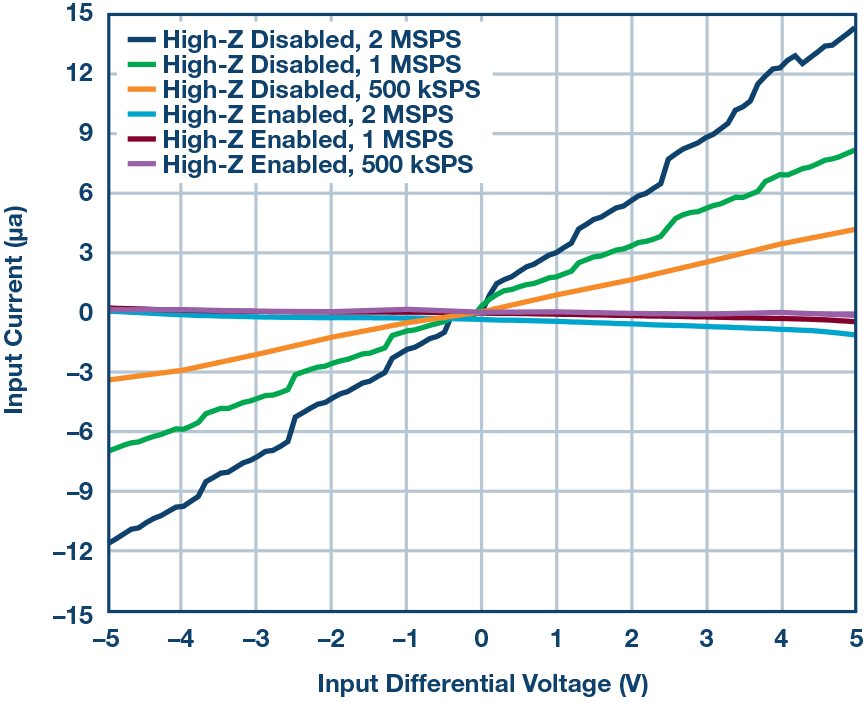
Figure 4 shows the input current of the AD4003/AD4007/AD4011 with high-Z mode enabled/disabled. The low input current makes the ADC a lot easier to drive than traditional SAR ADCs available in the market, even with high-Z mode disabled. If you compare the input current in Figure 4 with high-Z mode disabled against that of the previous generation AD7982 ADC, the AD4007 has reduced the input current by 4× at 1 MSPS. The input current reduces further to submicroampere range when high-Z mode is enabled.
With the reduced input current of this ADC family, it is capable of being driven with a much higher source impedance than traditional SARs. This means the resistor in the RC filter can have 10 times larger value than traditional SAR designs.
Precision Amplifiers Directly Drive the AD4000 ADC Family
For most systems, the front end, not the ADC itself, usually limits the overall ac/dc performance achievable by the signal chain. It’s evident from the selected precision amplifier’s data sheet in Figure 5 and Figure 6 that its own noise and distortion performance dominates the SNR and THD specification at a certain input frequency. However, this ADC family with high-Z mode allows a much expanded choice of driver amplifiers, including precision amplifiers used in signal conditioning stages, along with greater flexibility in the RC filter choice while still achieving optimal performance for the chosen amplifier.
Figure 5 and Figure 6 show the AD4003/AD4020 ADC’s SNR and THD performance using the low power ADA4692-2 (IQUIESCENT = 180 µA/amplifier), low input bias JFET ADA4610-1 (IQUIESCENT = 1.5 mA/amplifier), and zero-crossover distortion ADA4500-2 (IQUIESCENT = 1.55 mA/amplifier) precision amplifiers when driving the ADC inputs with a 1 kHz input tone using a 5 V reference at full throughput for both the high-Z enabled/disabled cases with various RC filter values. The ADA4692-2 and ADA4610-1 amplifiers achieve above 98 dB typical SNR with high-Z enabled for lower RC bandwidths of 260 kHz and 498 kHz, which helps remove wideband noise coming from the upstream signal chain components when the signal bandwidth of interest is low. Depending on applications requirements, the designers can select appropriate precision amplifier to drive the ADC inputs. For example, the ADA4692-2 rail-to-rail amplifier is better suited for a portable, power-sensitive applications that can directly drive this ADC family and still achieve optimal performance.
With high-Z mode enabled, the AD4003/AD4020 SNR is at least 10 dB better even for an RC bandwidth below 1.3 MHz with large R values greater than 390 Ω and THD holds up above –104 dB at an RC filter cutoff of 4.42 MHz using these amplifiers. Note that this ADC family can be oversampled by taking advantage of full throughput to achieve better SNR performance at lower RC filter cutoff.
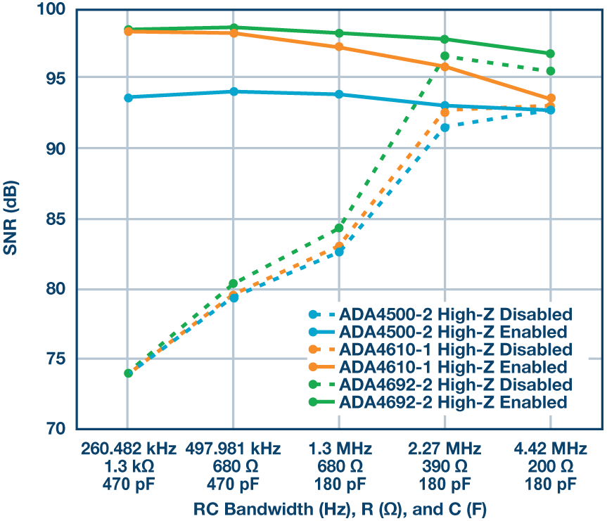
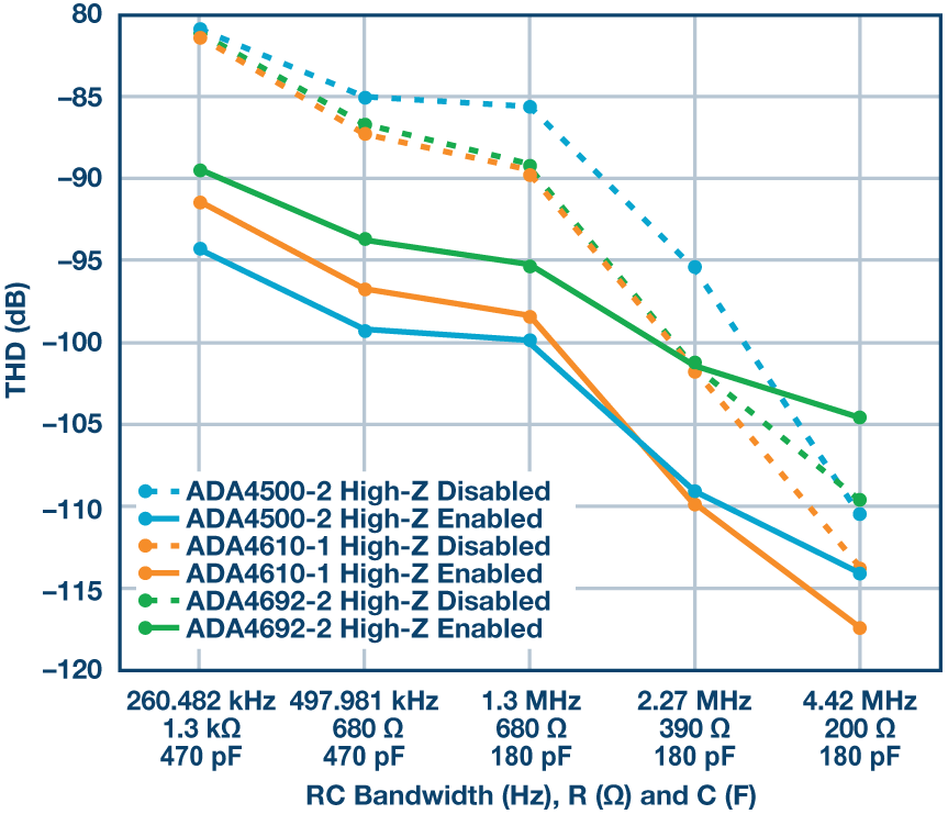
With high-Z enabled, the AD4003/AD4020 will consume typically 2 mW/MSPS to 2.5 mW/MSPS extra power, but this would still be significantly lower than using dedicated ADC drivers like the ADA4807-1, and this decision results in PCB area and BOM savings. System designers can use the 5.5× lower power ADC driver ADA4692-2 (vs. the ADA4807), and this ADC still achieves typical SINAD of about 96 dB when high-Z mode is disabled for 2.27 MHz and 4.47 MHz RC bandwidths. With high-Z mode enabled, the ADC SNR/THD performance is better using the ADC drivers, whereas with high-Z mode disabled, there is a trade-off between the ADC SNR/THD performance and RC filter cutoff.
Instrumentation Amplifier Directly Drives the AD4000 ADC Family
The instrumentation amplifiers offer excellent precision performance, common-mode rejection, and high input impedance to interface directly with sensors, but they have usually lower small signal bandwidth (<10 MHz). The customers designing precision signal chains (for example, ATE, medical equipment) with SAR ADCs and instrumentation amplifiers typically use signal conditioning or driver stage before the signal is fed to the ADC inputs for a level translation and a kickback settling purpose.
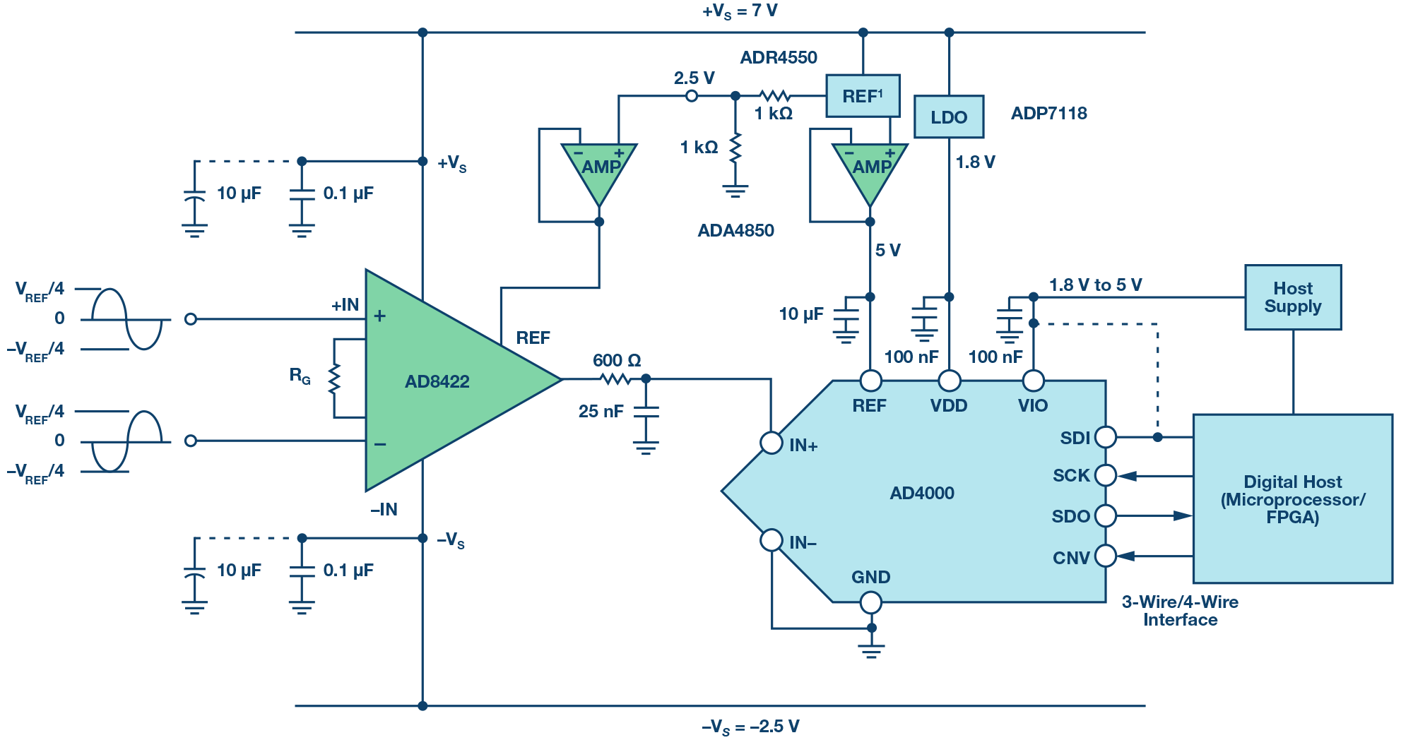
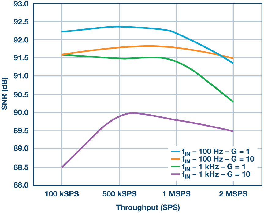
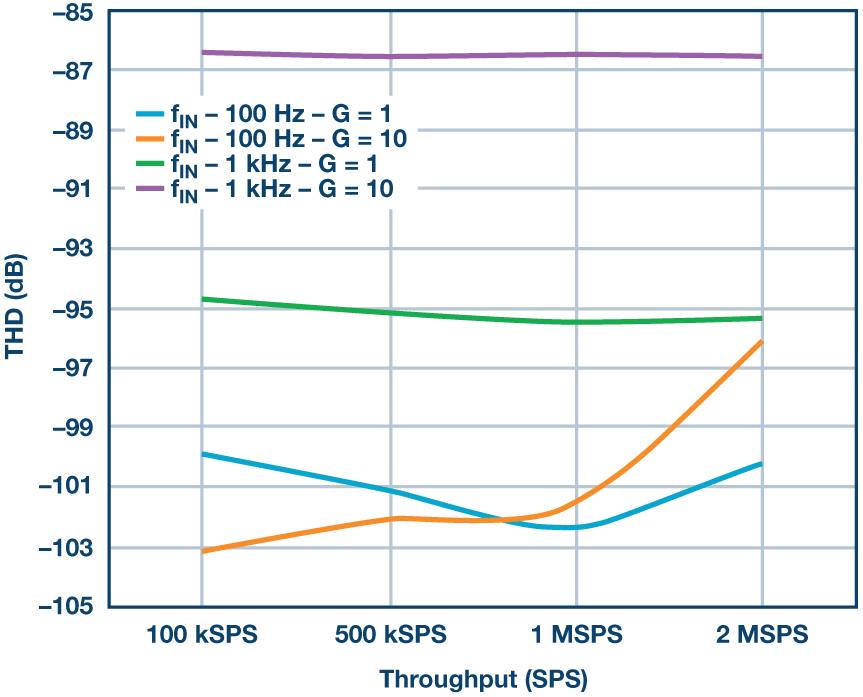
Figure 7 shows a simplified block diagram of the AD8422 directly driving the AD4000 when high-Z mode is enabled, which eliminates the driver stage and saves board space. The optimized RC filter values of 600 Ω and 25 nF are selected based on the bandwidth of interest to remove the wideband noise over 10 kHz. The REF pin of the AD8422 is biased to VREF/2 and buffered with the ADA4805 to achieve the optimized performance. This signal chain offers optimal SNR and THD performance for a 100 Hz and a 1 kHz input signal at gain (set by RG) of 1 (no RG) and 10 (RG = 2.2 kΩ). Figure 8 and Figure 9 show that with high-Z enabled, the ADC achieves SNR above 91 dB and THD above –96 dB for a gain of 1 and 10 with a 100 Hz input signal for every throughput up to 2 MSPS. As seen from Figure 8 and Figure 9, the SNR and THD get slightly better as the ADC throughput is reduced, offering longer acquisition time to settle the input kickback.
Conclusion
Table 1 shows the AD4000 family of pin-compatible, low power 16-/18-/20-bit precision SAR ADCs available in different speeds and input types that combines ease of use features with precision performance—enabling designers to solve the system-level technical challenges.
| Speed | 16-Bit, Single-Ended | 16-Bit, Differential | 18-Bit, Single-Ended | 18-Bit, Differential | 20-Bit, Differential |
| 2 MSPS | AD4000 | AD4001 | AD4002 | AD4003 | AD4020 |
| 1 MSPS | AD4004 | AD4005 | AD4006 | AD4007 | |
| 500 kSPS | AD4008 | AD4010 | AD4011 |
The AD4000 ADC family’s unique combination of high-Z mode, reduced input current, and longer acquisition phase enables ease of drive and helps designers eliminate a dedicated high speed ADC driver stage, which helps save PCB area, power, and BOM cost and also broadens their choice of ADC drivers. In addition, these traits allow designers to optimize RC filter values based on bandwidth of interest, which alleviates concerns for wideband noise, amplifier stability, ADC input protection, and dynamic power dissipation. This article has illustrated various use cases of precision amplifiers including instrumentation amplifier directly driving this ADC family inputs and it articulates how this family helps to solve common system-level issues without significantly compromising the precision performance.
参阅电路
1. Mathil Pachchigar and Alan Walsh. “Next-Generation SAR ADC Addresses Pain Points of Precision Data Acquisition Signal Chain Design.” Analog Dialogue, Vol. 50, December, 2016.