文章转自ADI官网,版权归属原作者一切
Introduction
In wireless base stations, the power amplifier (PA) dominates signal-chain performance in terms of power dissipation, linearity, efficiency, and cost. Monitoring and controlling the performance of a base station’s PA makes it possible to maximize the output power while achieving optimum linearity and efficiency. This article discusses the elements of a monitoring-and-control solution for the PA using discrete components—and describes an integrated solution.
Analog Devices has a suite of components that are ideally suited to such tasks. Multichannel digital-to-analog converters (DACs), analog-to-digital converters (ADCs), temperature sensors, and current sensors, as well as single-chip integrated solutions, are being applied in base stations to monitor and control a variety of analog signals. Discrete sensors and data converters provide maximum performance and configuration flexibility, while integrated solutions offer lower cost, smaller size, and higher reliability.
Optimizing a base station’s power efficiency is a key environmental consideration for companies in the telecom industry. Significant efforts are being made to reduce the overall energy consumption of base stations to lessen their impact on the environment. Electrical energy is the principal source of everyday operating costs in a base station, and the PA can be responsible for more than half of the power dissipation. Thus, optimizing the PA’s power efficiency improves operational performance, and provides environmental and financial benefits.
PA Control with Discrete Components
Figure 1 shows a basic power stage using a lateral-diffused metal-oxide semiconductor (LDMOS) transistor. The inherent trade-offs between linearity, efficiency, and gain determine the optimum bias condition for the PA transistor. Maintaining the drain bias current at an optimum value over temperature and time can significantly improve the overall performance of the PA, while ensuring that it stays within regulated output power levels. One way of controlling the gate bias current is to use a resistive divider to set the gate voltage at a fixed optimum value determined during evaluation.
Unfortunately, while this fixed-gate-voltage solution can be quite cost effective, it has a serious disadvantage: it does not correct for environmental changes, manufacturing spread, or supply-voltage variations. The two principal factors affecting the PA’s drain bias current are variations of the high-voltage supply line and the on-chip temperature.
A better approach is dynamic control of the PA gate voltage— using a digital control algorithm to measure the drain current, digitizing it with an ADC, and setting the required bias via a high-resolution DAC or a lower-resolution digital potentiometer. This control system allows the PA to maintain the required bias condition for optimized performance—set by a user-programmable setpoint—despite changes in voltage, temperature, and other environmental parameters.
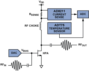
A key factor in this control approach is accurate measurement of the current furnished to the LDMOS transistor via the high-voltage supply line, using a high-side sensing resistor and an AD8211 current-sense amplifier. With a common-mode input range up to +65 V, the AD8211 provides a fixed gain of 20 V/V. The external sense-resistance sets the full-scale current reading. The amplifier output can be multiplexed into an ADC to generate digital data for monitoring and control. Care should be taken to ensure that the output voltage of the current-sense amplifier be as close as possible to the full-scale analog input range of the ADC. Constant monitoring of the high-voltage line enables the power amplifier to continuously readjust its gate voltage, even when voltage surges are sensed on the line, thus maintaining an optimum bias condition.
The drain-to-source current of the LDMOS transistor, IDS, as a function of the gate-to-source voltage, Vgs, has two temperature-dependent terms: the effective electron mobility, µ, and the threshold voltage, Vth.
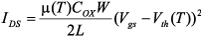
Vth and µ decrease with increasing temperature. Hence, temperature changes will cause variations in output power. Measuring ambient and internal temperatures of the PA using one or more ADT75 12-bit temperature sensors makes it possible to monitor the temperature variations on the board. The ADT75, a complete temperature monitoring system in an 8-lead MSOP package, offers ±1°C accuracy from 0°C to 70°C.
Multiplexing the voltage output of the temperature sensor, the drain current, and other data into an ADC allows temperature measurements to be converted into digital data for monitoring. Depending on the system configuration, it may be necessary to use a number of temperature sensors on the board. For example, if more than one PA is used—or if more than one predriver is required on the front end—a temperature sensor for each amplifier permits better control of the system. For monitoring both the current sensors and the temperature sensors, the AD7992, AD7994, and AD7998 multichannel 12-bit ADCs are useful for converting analog measurements into digital data.
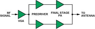
The digital information gathered from the current sensors and temperature sensors can be continuously monitored, using control logic or a microcontroller. Dynamic control of the PA gate voltage with a digital potentiometer or DAC—while monitoring the sensor readings and processing the digital data—allows an optimized biased condition to be maintained. The degree of control required on the gate voltage will determine the resolution of the DAC. Telecom companies commonly use multiple PAs in base station designs, as shown in Figure 2, to provide added flexibility in selecting a PA for each RF carrier and allow each PA to be optimized toward a particular modulation scheme. Also, combining parallel PA outputs provides improved linearity and overall efficiency. In such cases, the PAs may require multiple cascaded gain stages, including variable-gain amplifiers (VGAs) and predrivers, to meet the gain and efficiency requirements. A multichannel DAC can accommodate the various level-setting- and gain-control requirements of these blocks.
To achieve accurate PA gate control, the AD5622, AD5627, and AD5625 DACs offer 12-bit, single, dual, and quad outputs, respectively. They have internal buffers with excellent source- and sink capabilities, obviating the need for external buffers in most applications. The combination of low power, guaranteed monotonicity, and fast settling time make these parts ideal for accurate level-setting applications.
Where precision is not a primary specification and 8-bit resolution is acceptable, a digital potentiometer is a more cost-effective option. These digitally variable resistors perform the same electronic adjustment functions as mechanical potentiometers or variable resistors—but with enhanced resolution, solid-state reliability, and superior temperature performance. Nonvolatile and one-time-programmable (OTP) digital potentiometers are ideal in time-division duplexing (TDD) RF applications where the PA is turned off for the TDD receive period and turned on by a fixed gate voltage for the transmit period. This preprogrammed start-up voltage reduces the turn-on delay and improves efficiency in turning on the PA transistor for the transmit stage. The ability to turn off the PA transistor during the receive state prevents transmitter-circuit noise from corrupting the received signal and improves the overall efficiency of the PA. Depending on the number of channels, interface type, resolution, and the requirement for nonvolatile memory, a variety of digital potentiometers are available for this application. For example, the 256-position AD5172, a one-time-programmable, dual-channel, I2C®-compatible potentiometer, is well-suited for level-setting applications in RF amplifiers.
For monitoring and controlling gain with optimum linearity and efficiency, accurate measurement of the power levels of complex RF signals on the output of the PA is necessary. The AD8362 TruPowr™ rms power detector provides 65-dB dynamic range from 50 Hz to 3.8 GHz, allowing precise rms power measurement of RF signals typically found in W-CDMA, EDGE, and UMTS cellular base stations.
In Figure 3, the output of the power detector, VOUT, is connected to the gain-control terminal of the PA to adjust its gain. The PA output drives the antenna; the directional coupler picks up a fraction of the output, attenuates it appropriately, and applies it to the power detector. The output of the power detector, an rms measure of the transmitter output signal, is compared with the value programmed by the DAC, VSET; and the PA gain is adjusted to null difference. Thus, VSET sets the power gain precisely. The output of the ADC, a digital measure of VOUT , feeds into a larger feedback loop, which can track the transmitted power output, as measured by the AD8362, establishing the value of VSET and the system-determined gain requirement.
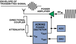
This method of gain control can be used with variable-gain amplifiers (VGAs) and variable-voltage amplifiers (VVAs) that are used in preceding stages of the signal chain. To measure both transmit- and receive power, the AD8364 dual detector simultaneously measures two complex input signals. In a system where a VGA or a predriver precedes the PA, and only one power detector is required, the gain on one of the devices is fixed, while VOUT feeds the control input of the other.
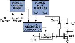
If the loop determines that the line current is too high, it sends a command to the DAC to reduce the gate voltage or shut down the part. In some applications, however, if voltage spikes or unacceptably high currents appear on the high-voltage supply line, the digital control loop cannot sense the high-side current, convert the signal to digital, and process the digital data by the external control logic rapidly enough to prevent device damage.
In an analog approach, an ADCMP371 comparator and an RF switch can be used to control the RF signal to the PA, as shown in Figure 4. The output voltage of the current sense is directly compared to the fixed voltage set up by the DAC. When a voltage higher than the fixed voltage appears at the output of the current sensor, due to a voltage or current spike, the comparator can toggle a control pin on the RF switch, cutting the RF signal to the gate of the PA almost instantaneously, preventing damage to the PA. This direct control, which bypasses the digital processing, is much faster and provides better protection.
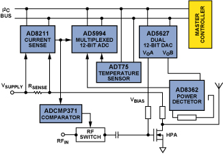
Combining the elements discussed above, a typical PA monitoring and control configuration, made up of discrete devices, is shown in Figure 5. In this case, the only amplifier being monitored and controlled is the PA itself, but a similar principle would apply to control of any of the amplifiers in the signal chain. All the discrete components are controlled using one master controller and operate off the same I2C bus.
Depending on the requirements of the signal chain, a number of amplifiers may be needed in the predrive and final stages to increase the overall power gain of the signal ahead of the antenna. Unfortunately, these additional power-gain stages have an adverse effect on the overall efficiency of the PA. To minimize the degradation of the PA’s efficiency, the drivers must be monitored and controlled to optimize performance. For example, the user would require a significant number of discrete components to monitor temperature, power, and voltage levels on the VGA, two predrivers, and two final-stage PAs used to gain up the signal in Figure 2.
Integrated Monitoring and Control
To solve this proliferation problem Analog Devices developed the AD7294, an integrated monitoring and control solution specifically designed to address this issue. The AD7294 contains all the functions and features required for general-purpose monitoring and control of current, voltage, and temperature—integrated onto a single chip.

The AD7294 consists of a 9-channel, 12-bit ADC and a 4-channel DAC having a sink/source capability of 10 mA. It is manufactured on 0.6-µm DMOS technology, which permits the current sensor to measure common-mode levels up to 59.4 V. The ADC has two dedicated current-sense channels, two channels for sensing external-junction temperatures, one channel for sensing the chip’s internal-temperature, and four uncommitted ADC inputs for general-purpose monitoring.
The ADC channels have the added benefit of hysteresis and high- and low-limit registers (which can also be found on the AD7992/AD7994/AD7998). The user can preprogram high- and low limits for an ADC channel; the monitored signal will flag an alert if these limits are violated. The hysteresis register gives the user the added capability of determining the reset point for the alert flag if a limit violation occurs. Hysteresis prevents a noisy temperature- or current-sensor reading from continuously toggling the alert flag.
Analog-to-digital conversions can be initiated in two different ways. The command mode allows the user to convert a single channel or a sequence of channels on demand. The autocycle mode converts automatically on a sequence of preprogrammed channels, an ideal mode of operation for system monitoring—especially for continuously monitoring signals, such as signal power and current sensing—and provides alerts only when the preprogrammed high- or low limits are violated.
Two bidirectional high-side current-sense amplifiers are provided (Figure 7). As the PA drain current flows through a shunt resistor, the small differential input voltage is amplified. The integrated current-sense amplifiers reject common-mode voltages up to 59.4 V and provide an amplified analog signal to one of the multiplexed ADC channels. Both current-sense amplifiers have a fixed gain of 12.5 and utilize an internal 2.5-V output-offset reference.
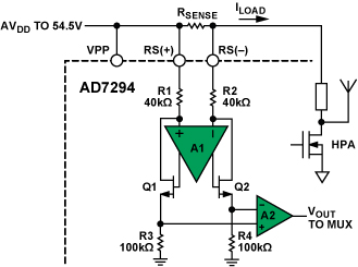
An analog comparator is provided with each amplifier for fault detection above a threshold of 1.2× full-scale voltage.
The four 12-bit DACs provide a digitally controlled voltage (with 1.2-mV resolution) to control the bias currents of the power transistors. They can also be used to provide control voltages for variable-gain amplifiers. The DAC core is a thin film, 12-bit, inherently monotonic string DAC with a 2.5-V reference and 5-V output span. Its output buffer drives the high-voltage output stage. The output range of the DAC, which is controlled by the offset input, can be positioned between 0 V and 15 V. This provides the end user the option of 12-bit-accurate control over a 5-V span, while allowing the flexibility of using bias voltages as high as 15 V, as PA transistors migrate to larger controlling-gate voltages. In addition, the ability of the four DACs to sink or source currents up to 10 mA makes external drive buffers unnecessary.
Conclusion
PA vendors are designing ever more complex PA front-end signal chains using a diversity of gain stages and control techniques. Available families of multichannel ADCs and DACs and analog RF components are ideally suited to address differing system partitions and architectures, allowing designers to implement cost-effective distributed control. Alternatively, single-chip solutions, such as the AD7294, provide significant advantages in terms of board area, system reliability, and cost. From a custom design perspective, the wealth of both dedicated-function- and integrated-system building blocks offer unprecedented empowerment to system designers.