文章转自ADI官网,版权归属原作者一切
Introduction
The broad acceptance of standards developed for the short range wireless connectivity market has been one of the notable features of the semiconductor market in the past few years. These standards include Bluetooth, the various flavors of Wi-Fi, ZigBee, and new emerging standards, such as Wibree/Bluetooth ULP and Ultra Wideband.
A sensible designer faced with the task of wirelessly connecting two or more devices will usually look to these standards for a solution, but the available wireless standards are not always the best fit for the application’s requirements.
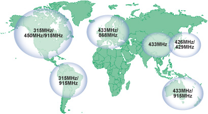
One reason is that these standards mainly specify operation in the license-free band at 2.4 GHz—due to its worldwide acceptance and approximately 84-MHz bandwidth. The 2.4-GHz band suffers from nontrivial coexistence issues and lower propagation distances for a given power budget, however, causing increased interest in the lower UHF bands. Common frequencies include 868 MHz and 433 MHz in Europe, 902 MHz to 928 MHz in the United States, and 426 MHz in Japan. These are usually collectively termed the sub-GHz bands, and they include other unlicensed bands below 1 GHz. Due to the shortage of wireless standards below 1 GHz, designers tend to use a proprietary physical layer (PHY) and communication protocol stack, which can then be tailored to their specific needs.
Figure 1 shows the locations where most of the unlicensed sub-GHz bands are utilized.
Simulation of Sub-GHz Wireless Connectivity Systems
The advantage of using a wireless standard like Wi-Fi or Bluetooth is that the standards working groups have already defined the data rate, modulation type, output power, and frequency plan, so designers need not be concerned with the underlying national regulations. Bluetooth designers, for example, can be confident that standard reference designs meet the maximum allowed radiated power, maximum modulation bandwidth, emission mask, and minimum number of hop channels to meet EN 300 440 and FCC Part 15 regulations covering the 2.4-GHz ISM band.
At sub-GHz frequencies, however, the problem is a little different. The fragmented nature of the bands results in fewer standards at sub-GHz, so most system designers operating at sub-GHz tend to use proprietary wireless protocols, exercising the freedom to choose the various system parameters themselves. The risk of doing so is that a given set of parameters may not meet national regulations. Thus, the ADI SRD Design Studio™ tool was developed to allow users to simulate various scenarios before going to the lab; it guides the user through the design process, while keeping the underlying regulations in mind. A graphical overview of the main tasks it performs is shown in Figure 2.
The range of subsystem operations and parameters to be considered in the development process includes PLL optimization, RF filtering and matching, data rate and modulation type, demodulation process, packet-data formatting, and average power consumption. System designers typically rely on a combination of spreadsheet-based tools and iterative lab work to help with the optimization of these parameters. Conventionally, time domain analysis can be performed using a SPICE-based simulator, but performing accurate phase-noise simulations in the frequency domain is usually possible only by using specialized software. Alternatively, designers can make multiple trips to a local regulatory test-house to optimize the system, but this can be expensive.
To help with these challenges, Analog Devices has released a free software package called ADI SRD Design Studio to allow real-time simulation and optimization of various system parameters using the ADF7xxx family of transceivers and transmitters. The development tool is based on the popular ADIsimPLL™ software, enhanced to allow users to view modulation in both the time and frequency domains using a virtual spectrum analyzer. Beyond this, ADI SRD Design Studio greatly simplifies the overall development process, creating a path along which a user can be guided and breaking down the design workflow into a number of distinct tasks, summarized in Table 1.
Table 1. List of tasks available in ADI SRD Design Studio.
| Task Name | Description | |
| 1 | New Design Wizard | Includes default settings for the various regional regulations (FCC, ETSI, ARIB, etc.). |
| 2 | link Budget | Allows range estimation using different propagation models and fade margins. |
| 3 | Frequencies Worksheet | Aids in choice of XTAL and PFD for various combinations of data rates and frequencies. |
| 4 | Transmitter Spectrum | Extremely flexible spectrum analyzer (FFT based). |
| 5 | Packet Formatting | Enter in your packet structure to see effect on battery life and packet error rate (PER). |
| 6 | Sync Detection | Helps choose sync byte with good auto correction properties to minimize false triggers. |
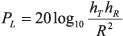
| 7 | Power Consumption | Different sleep-Tx-Rx scenarios possible. Used for battery life calculation. |
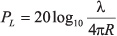
| 8 | Schematic | Gives external schematic based on system parameters (for example, loop filter, VCO inductor, XTAL, and matching). |
Basic Overview of Operation
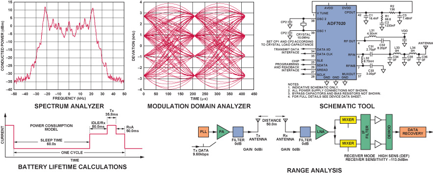
The core of ADI SRD Design Studio is a library of ADF7xxx device models that contains parameterized data for each device, including, for example, the VCO and synthesizer phase noise, VCO gain, frequency range, available data-filter types, sensitivity, and noise figure. Using these models, a nonlinear time-domain analysis is performed with the baseband data used to modulate the RF carrier to obtain a time-series output of the VCO. The baseband data can be chosen to be pseudorandom (PRBS) or a periodic (010101) pattern. Unlike conventional linear analysis, nonlinear effects like VCO pulling, nonlinear VCO gain curves, and charge-pump saturation are accurately modeled. An FFT is then performed on the time domain waveform to obtain the spectrum-analyzer output.
The versatile spectrum analyzer allows the user to adjust resolution bandwidth, detector type, and number of sweeps like a commercial spectrum analyzer. The resolution bandwidth can be set from 100 Hz to 300 kHz, while the span is selectable from 1 kHz to 3 MHz. Users can also choose whether to use peak- or average detectors, instructing the analyzer to take the maximum or average number, respectively, in each FFT bin. Having these parameters adjustable is useful because each regulatory standard specifies different measurement conditions—including the resolution bandwidth, span, and detector type that should be used in the measurement equipment. The simulator takes all of these into account in the various preset tests available in the spectrum analyzer mode. These useful preset tests, listed in Table 2, mean that users can quickly test to the relevant standard without poring over the documentation.
Table 2. List of preset measurements in spectrum-analyzer mode.
| Test # | Regulation | Preset Measurement |
| 1 | ETSI EN 300 220 | Modulation Bandwidth |
| 2 | ETSI EN 300 220 | Adjacent Channel Power |
| 3 | ETSI EN 300 220 | Occupied Bandwidth |
| 4 | FCC 15.231 | –20 dB Bandwidth |
| 5 | FCC 15.247 | –20 dB Bandwidth |
| 6 | FCC 15.247 | –6 dB Bandwidth |
| 7 | FCC 15.247 | 3 kHz Power Spectral Density |
| 8 | FCC 90.210 | Emission Mask D |
| 9 | FCC 15.249 | –20 dB Bandwidth |
| 10 | FCC 15.231 (b) | Field Strength |
| 11 | FCC 15.231 (e) | Field Strength |
| 12 | ARIB STD-T67 | Occupied Bandwidth (25 kHz) |
| 13 | ARIB STD-T67 | Occupied Bandwidth (12.5 kHz) |
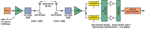
In addition to the transient- and spectrum-analyzer modes, a PLL frequency-domain analysis is performed to calculate PLL loop filter components and estimate phase- and gain margin. By adjusting the PLL loop bandwidth in the simulation, users can see the effect on the transmit modulation spectrum and phase-plot eye opening. This allows a proper optimization of the loop filter without having to rely on a small subset of vendor filter tables or basic guidelines. All three of these main simulations run in less than two seconds in a typical setup.
Propagation Models
One of the other useful tools in the ADI SRD Design Studio package is the link-analysis worksheet, which is used to estimate link budget and range under various conditions. Like all of the other tasks, it is integrated into the main simulator. A change in the data rate to conform to an emission mask will cause a corresponding change in sensitivity, affecting the link budget and ultimately the propagation range. This capability provides an advantage over a set of standalone tools, as a change in one parameter—such as data rate—will ripple through to the other worksheets.
The link analysis first calculates the link budget, that is, the difference between the transmit power and the receive sensitivity, taking any filter- or antenna loss into account. The device setup for this simulation is shown in Figure 3.
The range can then be determined by increasing the distance between the antennas in the simulation until the path loss equals the link budget, that is the point at which the link margin is 0 dB. The path loss is calculated using a user-selected propagation model; three different propagation models are supported: free-space, over-ground, and simple-indoor.
A. Free-Space Propagation Model
The free-space model assumes that there are no obstructions, nor any significant reflecting objects (including the ground), between the transmitter and receiver. With spacing between transmitter and receiver, R, wavelength, λ, and path loss, PL, the following formula tends to give optimistic propagation ranges for most practical emitter/receiver placements.
B. Over-Ground Propagation Model
Here, the transmitter is at height, hT, above flat ground, the receiver is at height, hR, and the spacing is R. This formula gives quite accurate results for clear line-of-sight (LOS) conditions—for example, on a beach or a relatively wide piece of road. This simulation shows that propagation ranges of greater than 3 km are possible using the ADF7xxx devices, without the need for an external power amplifier (PA) or low-noise amplifier (LNA).
C. Simple-Indoor Propagation Model
where P0 is the path loss at 1 m, and n is an exponent whose value depends on the environment. Reference 3 lists some reported values for n in various environments, such as a factory floor, multistory office building, etc. Most designers simply insert a value of n based on empirical results.
Another useful task in ADI SRD Design Studio is the packet-formatting worksheet. This allows users to input a given packet format and see the effect of packet length on battery life, choose a sync word that will result in low false-trigger probability, and translate the bit error rate (BER) into a corresponding packet error rate (PER), based on the packet length. The BER-to-PER conversion is useful because some IC vendors specify sensitivity in terms of BER—and others specify it in terms of PER.
Testing a Simulation Setup in the Lab
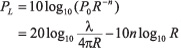
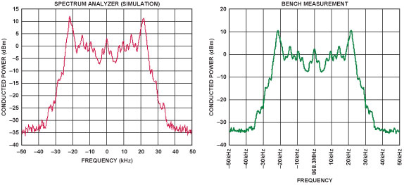
once the simulation has been completed and the results are acceptable, the file can be saved and the simulation settings exported to the Analog Devices ADF7xxx programming software. Then, a bench test can be run using the program device utility. This function will export the frequency, data rate, modulation type, etc. to the ADF7xxx programming software—which will allow quick device configuration in the lab. Bench measurements compare quite well with simulated results, as shown in Figure 4. The simulated and bench measurements for a 9.6-kbps GFSK signal at 868 MHz agree quite closely. When running these comparisons, care should be taken that the simulator uses the same PLL loop filter as on the board, as it will affect the shape of the output spectrum.
Summary
ADI SRD Design Studio was released in July 2007, and has received over 5,000 downloads at the time of this writing. Because Analog Devices is committed to improving the software, an online forum allows users to post suspected bugs, issues, or suggestions for the next revision of the software. This forum is hosted on the Radiolab website, which can be accessed via ADI SRD Design Studio. Users should also check this website periodically for patches or upgrades to the software.
New wireless devices will be added to the software tool as Analog Devices expands its portfolio, including devices at different frequencies—and supporting different modulation schemes. ADI SRD Design Studio should become a very useful part of the wireless connectivity designer’s toolkit and a must for anyone designing with the Analog Devices ADF7xxx family of transmitters or transceivers.
参阅电路
Analog Devices website: www.analog.com/srddesign.
Harney, A. and C. O’Mahony. “Wireless Short-Range Devices: Designing a Global License-Free System for Frequencies < 1 GHz.” Analog Dialogue. Vol. 40, No. 1. March 2006. pp. 18–22.
Hashemi, H. “The Indoor Radio Propagation Channel.” Proc. IEEE. Vol. 81, No. 7. July 1993. pp. 943–968.