LTC3315B相关信息来自ADI官网,详细参数以官网发布为准,LTC3315B供给信息可在查IC网查找相关供给商。
产品概况
The LTC3315B features dual 2A monolithic synchronous step-down converters operating from a 2.25V to 5.5V input supply in one package for space-constrained applications with demanding performance requirements. Using constant frequency, peak current mode control at switching frequencies up to 10MHz with a minimum on-time as low as 25ns, both bucks achieve high efficiency and fast transient response in a very small application footprint.
The LTC3315B operates in forced continuous or pulse skip mode for low noise or in Burst Mode® operation for high efficiency at light loads. The common buck switching frequency is 6MHz and can be synchronized to an external oscillator via the MODE/SYNC pin.
The LTC3315B can regulate outputs as low as 500mV. Other features include precision enable thresholds, a PGOOD signal, output overvoltage protection, thermal shutdown, output short-circuit protection, and up to 100% duty cycle operation for low dropout. The LTC3315B is available in a compact 2mm × 2mm LQFN package.
Applications
- Servers, Telecom Supplies, Optical Networking
- Distributed DC Power Systems (POL)
- FPGA, ASIC, µP Core Supplies
- Industrial/Automotive/Communications
优势和特色
- Dual Outputs Each with 2A Output Current
- High Efficiency: 19mΩ NMOS and 75mΩ PMOS
- Wide Bandwidth, Fast Transient Response
- Switching Frequency Synchronizable Up to 10MHz
- VIN Range: 2.25V to 5.5V
- VOUT Range: 0.5V to VIN
- VOUT Accuracy: ±1%
- Low Ripple Burst Mode® Operation
- Peak Current Mode Control
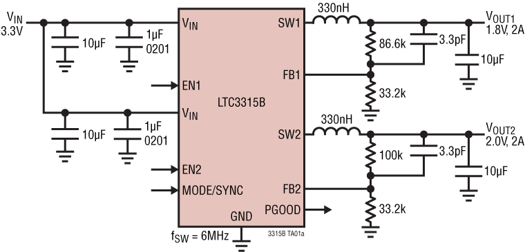
LTC3315B电路图
LTC3315B中文PDF下载地址
LTC3315B下载链接地址:https://www.analog.com/media/en/technical-documentation/data-sheets/ltc3315b.pdf