ST公司的stm32F334x4/6/8系列MCU是根据高性能ARM 32位CortexR-M4 RISC核,作业频率高达72MHz,并嵌入了浮点单元(FPU),一起集成了高达64KB闪存和12KB SRAM的嵌入存储器,以及连接到两条APB总线的各种增强I/O和外设.本文介绍了STM32F334x4/6/8首要特性,框图和时钟树, STM32F334 Discovery板首要特性,框图,电路图,PCB元件布局图和资料清单.
The STM32F334x4/6/8 family is based on the high-performance ARM 32-bit CortexR-M4 RISC core operaTIng at a frequency of up to 72 MHz, and embedding a floaTIng point unit (FPU). The STM32F334x4/6/8 family incorporates high-speed embedded memories (up to 64 Kbytes of Flash memory, up to 12 Kbytes of SRAM), and an extensive range of enhanced I/Os and peripherals connected to two APB buses.
The STM32F334x4/6/8 devices offer a High resoluTIon TImer,two fast 12-bit ADCs (5 Msps), up to three ultra-fast comparators, an operational amplifier, three DAC channels, a lowpower RTC, one high-resolution timer, one general-purpose 32-bit timer, one timer dedicated to motor control, and four general-purpose 16-bit timers. They also feature standard and advanced communication interfaces: one I2C, one SPI, up to three USARTs and one CAN.
The STM32F334x4/6/8 family operates in the –40 to +85 ℃ and –40 to +105 ℃ temperature ranges from a 2.0 to 3.6 V power supply. A comprehensive set of power-saving mode allows the design of low-power applications.
The STM32F334x4/6/8 family offers devices in 32, 48 and 64-pin packages.
STM32F334x4/6/8首要特性:
• Core: ARMR-32-bit-CortexR-M4 CPU with FPU (72 MHz max), single-cycle multiplication and HW division, and DSP instruction
• Memories
– Up to 64 KB of Flash memory
– Up to 12 KB of SRAM with HW parity check
– Routine booster: 4 KB of SRAM on instruction and data bus with HW parity check (CCM)
• CRC calculation unit
• Reset and supply management
– VDD,VDDA voltage range: 2.0 to 3.6 V
– Power-on/Power-down reset (POR/PDR)
– Programmable voltage detector (PVD)
– Low-power modes: Sleep,Stop,Standby
– VBAT supply for RTC and backup registers
• Clock management
– 4 to 32 MHz crystal oscillator
– 32 kHz oscillator for RTC with calibration
– Internal 8 MHz RC (up to 64 MHz with PLL option)
– Internal 40 kHz oscillator
• Up to 51fast I/O ports, all mappable on external interrupt vectors, several 5 V-tolerant
• 7-channel DMA controller
• Up to two ADC 0.20 μs (up to 21 channels) with selectable resolution of 12/10/8/6 bits, 0 to
3.6 V conversion range, singleended/ differential mode, separate analog supply from 2.0 to 3.6 V
• Temperature sensor
• Up to three 12-bit DAC channels with analog supply from 2.4 V to 3.6 V
• Three ultra-fast rail-to-rail analog comparators with analog supply from 2 V to 3.6 V
• One operational amplifiers that can be used in PGA mode, all terminals accessible with analog supply from 2.4 to 3.6 V
• Up to 18 capacitive sensing channels supporting touchkeys, linear and rotary touch sensors
• Up to 12 timers
– HRTIM: 6 x16-bit counters, 217 ps resolution, 10 PWM, 5 fault inputs, 10 ext event input, 1 synchro. input,1 synchro. out
– One 32-bit timer and one 16-bit timer with up to 4 IC/OC/PWM or pulse counter and quadrature (incremental) encoder input
– One 16-bit 6-channel advanced-control timer, with up to 6 PWM channels, deadtime generation and emergency stop
– One 16-bit timer with 2 IC/OCs, 1 OCN/PWM, deadtime generation, emergency stop
– Two 16-bit timers with IC/OC/OCN/PWM, deadtime generation and emergency stop
– Two watchdog timers (independent, window)
– SysTick timer: 24-bit downcounter
– Up to two 16-bit basic timers to drive the DAC
• Calendar RTC with alarm, periodic wakeup from Stop
• Communication interfaces
– CAN interface (2.0 B Active)
– One I2C with 20 mA current sink to support Fast mode plus, SMBus/PMBus
– Up to 3 USARTs, one with ISO/IEC 7816 interface, LIN, IrDA, modem control
– One SPI
• Debug mode: serial wire debug (SWD), JTAG
• 96-bit unique ID
• All packages ECOPACKR2
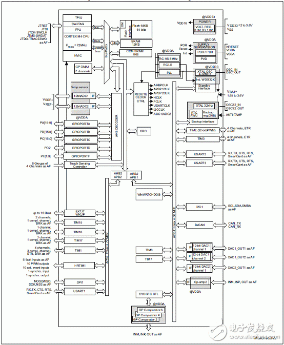
图1. STM32F334x4/6/8框图

图2. STM32F334x4/6/8时钟树框图
STM32F334 Discovery板32F3348DISCOVERY
Discovery kit for STM32F3 series with STM32F334C8 MCU
The STM32F334 discovery kit (32F3348DISCOVERY) helps you to discover the full features of the STM32F3x4 line and to develop your applications. It is based on an STM32F334C8T6 and includes an ST-LINK/V2-1 embedded debug tool interface, high brightness LED dimming with buck converter, buck/boost converter, LEDs, pushbuttons.
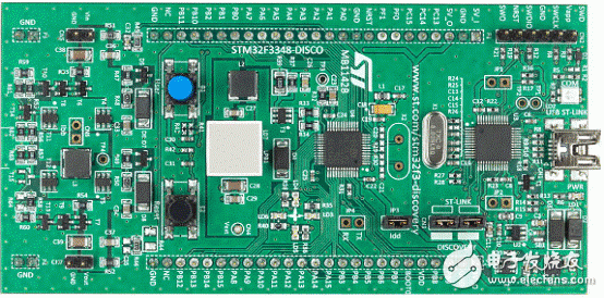
图3.STM32F334 Discovery板32F3348DISCOVERY外形图
STM32F334 Discovery板首要特性:
The STM32F334 discovery board offers the following features:
• STM32F334C8T6 microcontroller featuring 64 KB of flash memory, 16 KB of RAM in an LQFP48 package
• On-board ST-LINK/V2-1 with selection mode switch to use the kit as a standalone ST-LINK/V2-1 (with SWD connector for programming and debugging)
• USB re-enumeration capability: three different interfaces supported on USB – Virtual com port – Mass storage – Debug port
• Board power supply: through USB bus or from an external 5 V supply voltage
• External application power supply: 3 V and 5 V
• High brightness LED dimming with buck converter
• One buck/boost converter
• Six LEDs:
– LD1 (red) for 3.3 V power on
– LD2 (red/green) for USB communication
– Four user LEDs: LD3 (red), LD4 (orange), LD5 (green) and LD6 (blue).
• Two pushbuttons (user and reset).
• Extension header for LQFP48 I/Os for a quick connection to the prototyping board and easy probing.
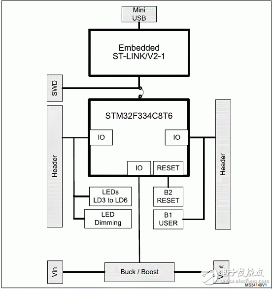
图4.STM32F334 Discovery板硬件框图
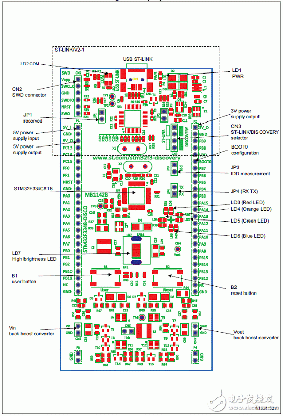
图5.STM32F334 Discovery板元件分布图:顶层

图6.STM32F334 Discovery板元件分布图:底层
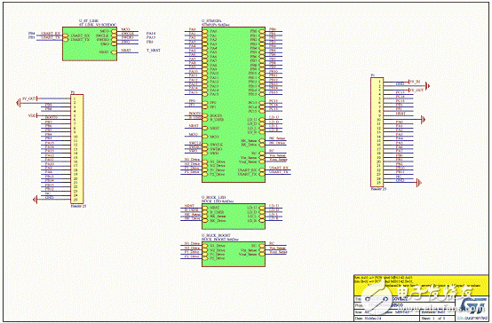
图7.STM32F334 Discovery板电路图(1)
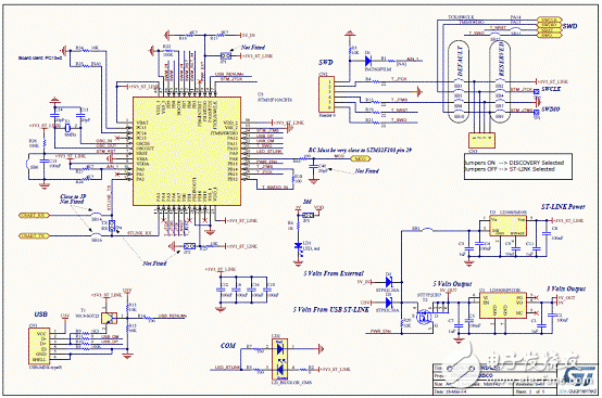
图8.STM32F334 Discovery板电路图(2)

图9.STM32F334 Discovery板电路图(3)
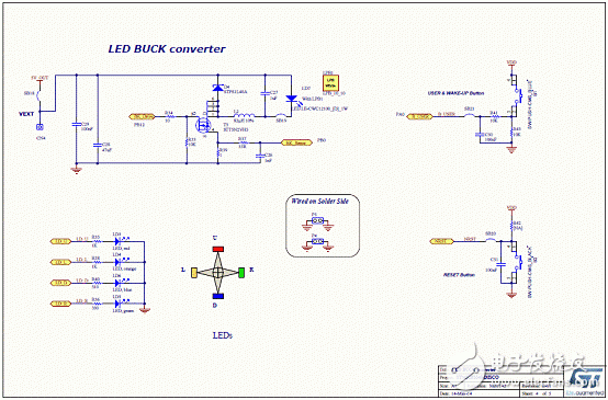
图10.STM32F334 Discovery板电路图(4)
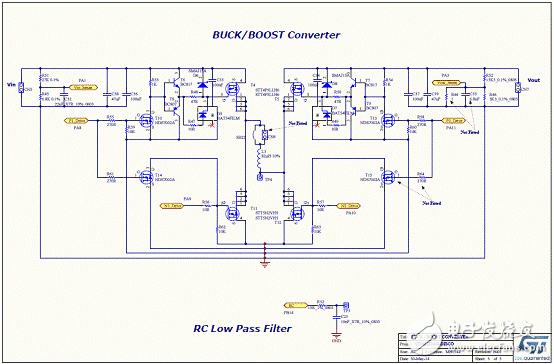
图11.STM32F334 Discovery板电路图(5)