文章转自ADI官网,版权归属原作者一切
Introduction
High-availability systems, such as servers, network switches, redundant-array-of-independent-disk (RAID) storage, and other forms of communications infrastructure, need to be designed for near-zero downtime throughout their useful life. If a component of such a system fails or needs updating, it must be replaced without interrupting the rest of the system. The board or module will have to be removed—and its replacement plugged in—while the system remains up and running. This process is known as hot swapping, or in some cases hot plugging (where the module interacts with the system software). To hot swap safely, connectors with staggered pins are often used to ensure that grounds and local power are established before other connections are made. In addition, each printed-circuit board (PCB) or plug-in module has an on-board hot-swap controller to facilitate the safe removal and insertion of the module from a live backplane. While in operation, the controller also offers continuous protection from short circuits and overcurrent faults.
Although the currents that must be interrupted and started up can be large, some of the subtleties of high-current design are often given very little consideration. Since the “devil is in the details,” this article will focus on the function and significance of the components of a hot-swap control circuit—and provide an in-depth look at design considerations and optimum component selection criteria in the design process using an Analog Devices ADM1177 hot-swap controller.
Hot-Swap Topologies
The two system-power levels commonly found in high-availability systems, –48 V and +12 V, use different configurations for hot-swap protection. The –48-V system incorporates low-side hot-swap control and pass-MOSFET; +12-V systems use a high-side controller and pass-MOSFET.
The –48-V approach originated in traditional telecommunications-exchange system technology. Examples can be seen in Advanced Telecommunications Computing Architecture (ATCA) systems, optical networks, base stations, and blade servers. As a voltage commonly obtained from battery stacks, 48 V was chosen because power and signals could be transmitted over distance without significant losses, yet the level is not high enough to risk severe electric shock under ordinary conditions. Negative polarity was chosen because, in the inevitable presence of moisture when exposed to the elements, the migration of metallic ions from anode to cathode is far less corrosive with the positive terminal grounded.
In data communications systems, however, where distance is not an important factor, the +12-V supply is more reasonable, making it popular in blade-server and network-system designs. This article will concentrate on +12-V systems.
The Hot-Swap Event
Consider a system with a 12-V backplane and a rack of removable modules. Each module must have the ability to be withdrawn and replaced without affecting the normal operation of any of the adjacent modules in the rack. In the absence of a controller, each of the modules may present a considerable amount of load capacitance to the supply line, usually of the order of millifarads. When a module is first inserted, its uncharged capacitors demand as much current as is available to charge up the load. If this inrush current is not limited, it could reduce terminal voltages, causing a significant brownout on the main backplane, resetting many of the adjacent modules on the system, and damaging the module’s connectors due to the high initial current.
This can be resolved with a hot-swap controller (Figure 1), which carefully controls the inrush current to ensure a safe power-up interval. The hot-swap controller will also continually monitor the supply current after power-up for protection against short circuits and overcurrent conditions during normal operation.
The Hot-Swap Controller
The ADM1177 hot-swap controller consists of three main components (Figure 2): an N-channel MOSFET that serves as the main power-control switch, a sense resistor that measures the current, and the hot-swap controller—which includes a current-sense amplifier—completing the loop to control the MOSFET’s pass current.
Inside the hot-swap controller, a current-sense amplifier monitors the voltage drop across the external sense resistor. This small voltage (typically ranging from 0 mV to 100 mV) must be amplified to a useful level. The amplifier gain in the ADM1177 is 10, so, for example, a 100-mV drop produced by a given amount of current will be amplified to 1 V. This voltage is compared to a fixed or variable reference voltage. With a 1-V reference, a current that produces a voltage greater than 100 mV (±3%) across the shunt will cause the comparator to indicate an overcurrent. The maximum-current trip point is thus principally determined by the shunt resistance, the amplifier gain, and the reference voltage; the shunt resistance value sets the maximum current. A TIMER circuit sets a limit to the length of time a given overcurrent condition can exist.
The ADM1177 has a soft-start function in which the overcurrent reference is ramped up linearly rather than turned on abruptly, forcing the load current to follow in a similar manner. This is achieved by injecting current from an internal current source into an external capacitor (SS pin) to linearly ramp the comparator’s reference input from 0 V to 1 V. The external SS capacitor sets the rate of this ramp. If necessary, the SS pin can also be driven directly by voltage to set the maximum current limit.
An ON circuit, consisting of a comparator and reference circuit, enables the device. It accurately programs the voltage that the supply must reach to enable the controller. once the device is enabled, the gate begins to charge up. The gate of the N-channel MOSFET used in this type of circuit must be above the source. In order to achieve this over the range of supply voltage (VCC), the hot-swap controller has an integrated charge pump capable of maintaining the GATE pin as much as 10 V higher than VCC. The GATE pin requires a charge-pumped pull-up current to enable the MOSFET and pull-down currents to disable the MOSFET when necessary. Weak pull-down currents are used for regulation, and stronger pull-down currents are used to quickly disable the MOSFET in the event of a short circuit.
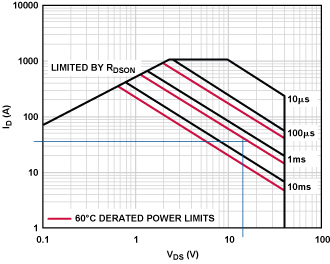
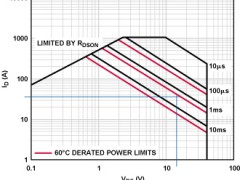
The final essential block of the hot-swap controller is the TIMER, which limits the time the current is in regulation during an overcurrent event. MOSFETs are designed to withstand a given amount of power for a prescribed maximum time. The MOSFET manufacturers outline this range, or safe operating area (SOA), using a graph such as that shown in Figure 3.
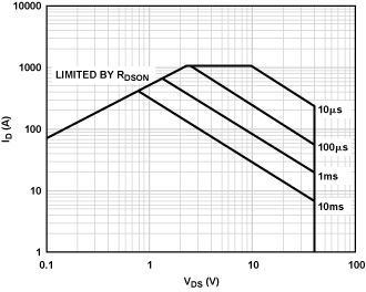
The SOA graph shows a relationship between the combined drain-source voltage, drain current, and the time duration that the MOSFET can withstand this dissipation. For example, the MOSFET in Figure 3 can withstand 10 V and 85 A (850 W) for 1 ms. If this condition persists for a greater duration, the MOSFET will be destroyed. The TIMER circuit can ensure that the length of time the MOSFET is subject to these worst-case conditions is limited by the external TIMER capacitor. For example, if the TIMER was set to 1 ms and the current exceeded the limit for more than 1 ms, the circuit would time out and shut down the MOSFET.
In the ADM1177, to provide a margin of safety, the TIMER current-sense voltage activation threshold is set to 92 mV. The hot-swap controller will thus start timing the current conservatively as the sense voltage approaches the regulated value of 100 mV.
Design Example
Because of the flexibility permitted by the design of controllers like the ADM1177, it may be useful to demonstrate how one would be applied in a 12-V hot-swap design example. The following conditions are assumed for this example:
Controller is the ADM1177
- VIN = 12 V (±10%)
- VMAX = 13.2 V
- ITRIP = 30 A
- CLOAD = 2000 μF
- VON = 10 V (a good supply level to switch on the controller)
- IPOWERUP = 1 A (dc bias current required by the load during power-up)
To simplify this discussion, the calculations exclude the effects of component tolerances. These tolerances should of course be considered when designing for worst-case conditions.
ON Pin
Consider first the condition to enable the controller when the supply voltage exceeds 10 V. If the threshold of the ON pin is 1.3 V, the voltage-divider ratio from VIN to the ON pin needs to be 0.13:1. For accuracy, the pin leakage current should be taken into account when selecting the resistance of the string.
A resistive divider consisting of 10-kohm and 1.5 kohm resistors will have a suitable ratio of 0.130.
Sense-Resistor Selection
The sense resistor is chosen based on the load current required to start the TIMER.
where VSENSETIMER = 92 mV.
The maximum power dissipated by the sense resistor at 30 A is
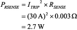
So the sense resistor should be capable of dissipating 3 W. If a single resistor with the correct power rating or resistance is not available, the sense resistor can be made with multiple resistors.
Load Capacitance Charge Time
The time it takes to charge the load capacitance must be determined prior to selecting the MOSFET. During the power-up phase, the controller will usually hit the current limit due to the inrush current demanded by the load capacitance. If the time set by the TIMER pin is insufficient to allow the load capacitors to charge, then the MOSFET will be disabled and the system will not power up. We can use the following equation to determine the ideal value:
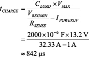
where VREGMIN = 97 mV, the minimum regulation voltage of the hot-swap controller.
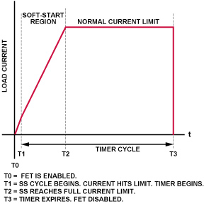
This equation assumes an ideal condition of load current ramping from 0 A to 30 A instantaneously. In reality, the gate charge, QGS, of larger MOSFETs serves to limit the slew rate of the gate voltage—and hence the power-up current profile—so that a quantity of charge is delivered to the load capacitor without triggering the TIMER function. In Figure 4, the MOSFET with the higher QGS results in the TIMER being active for a shorter period, T1 to T3, as compared to the MOSFET with the lower QGS, which causes the timer to be active during T0 to T2.
This is because the charge delivered between T0 and T1 accumulates at less than the current limit. Thus, the calculated time required can be reduced accordingly. This amount is difficult to quantify; it depends on the controller gate current and MOSFET specification for gate charge and capacitances. Since it may account for as much as 30% of the total charge current in some cases, it needs to be considered, particularly in designs using large MOSFETs and high currents.
For designs using MOSFETs with lower gate charge, a fast gate ramp can be assumed. This will result in a fast ramp from 0 A to ITRIP, which may cause unwanted transients; in this case, soft start should be used.
Soft Start
With soft start, the inrush current is linearly ramped from zero to full scale over a period of time set by the SS capacitor. This will provide an inrush ramp that avoids the sudden impact of the 30-A limit, and is accomplished by ramping up the reference current. Note that the current is in regulation during the SS event, and therefore the TIMER is active from the moment the soft start begins, as can be seen in Figure 5.
Therefore, a soft-start time of no more than 10% to 20% of the total TIMER is recommended. For this example, we can choose a time of 100 μs. The SS capacitance value can be determined as follows:
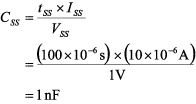
where ISS = 10 μA and VSS = 1 V.
MOSFET and TIMER Selection
The first step to choosing a suitable MOSFET is to select the VDS and ID criteria. For a 12-V system, VDS should be 30 V or 40 V to handle transients that could destroy the MOSFET. The ID of the MOSFET should be much larger than the required maximum (see the SOA graph in Figure 3). In high-current applications, one of the most important specifications will be the MOSFET’s RDSON. Low values of this parameter will ensure that minimum power is lost in the MOSFET when it is fully enhanced in normal operation—and that minimal heat is generated at full load.
Thermal and Power Considerations
Before considering the SOA specifics and TIMER selection, the power dissipation of the MOSFET at full dc load needs to be considered because overheating must be avoided. As the temperature of the MOSFET increases, its power rating is reduced, or derated. In addition, running MOSFETs at high temperatures decreases their life span.
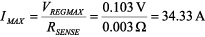
Recall that the hot-swap controller initiates the TIMER at a minimum sense voltage of 92 mV. For this calculation, we need to know the maximum possible dc current that can flow without tripping the TIMER. Assume the worst-case VREGMIN of 97 mV. Then,
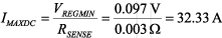
Assuming that the MOSFET’s maximum RDSON is 2 milliohms, the power is
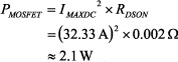
The MOSFET’s thermal resistance at ambient temperature will be specified in the data sheet. The footprint size and additional copper will have an effect on this value. Assume

As the MOSFET is required to dissipate 2.1 W, a worst-case temperature rise of 126°C above ambient can be expected:
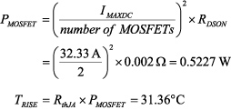
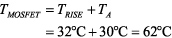
One way to reduce this number is to use two or more MOSFETs in parallel. This will effectively reduce the RDSON and thus the power dissipation in the MOSFETs. With two MOSFETs, a maximum temperature rise of 32°C per MOSFET will be incurred, assuming current is divided evenly between the devices (some tolerance should be allowed). The following shows the power in each MOSFET:
With this temperature rise and an assumed ambient temperature of TA = 30°C, a maximum case temperature of 62°C can be expected for each MOSFET.
MOSFET SOA Considerations
The next step is to review the SOA graphs to find a suitable MOSFET to handle worst-case conditions. In the worst-case short-circuit-to-ground condition, VDS can be assumed to be the VMAX of 13.2 V, as this will be the maximum voltage present across the MOSFET with its source terminal pulled to GND. In regulation, the worst case will be based on the maximum data sheet specification for the hot-swap controller regulation point. This is equal to 103 mV. The current can then be calculated as follows:
Before comparing this to the MOSFET SOA graphs, we need to consider the temperature derating of the MOSFET, since the SOA graph is based on data at ambient case temperature, TC = 25°C. First calculate the power dissipation at TC = 25°C:
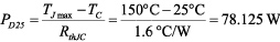
where RthJC is specified in MOSFET data sheet.
Now perform the same calculation for TC = 62°C:
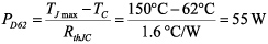
Thus, a derating factor of 1.42 is calculated as follows:
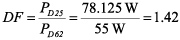
This needs to be applied to the SOA graph, of the MOSFET in Figure 3. The diagonal lines that represent the time maximum power is applied need to be moved downward to reflect the adjusted power ratings.
We earlier used the 1-ms line as an example to illustrate how the curves work. For example, take a point on that line—say (20 A, 40 V); the power at that point is 800 W. Applying the derating formula:
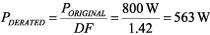
At 40 V, the corresponding current for derated power is 14 A. Plotting this point on the SOA graph establishes a point on the new 62°C-derated 1-ms line. New 10-ms and 100-μs lines can be established in the same way. The new lines are shown in red in Figure 6.
Selecting the TIMER Capacitor
The SOA’s new derating lines can be used to recalculate the TIMER value. Draw a horizontal line from IMAX ≈ 35 A and a vertical line from VMAX = 13.2 V (faint blue lines), then determine their intersection point with respect to the red lines. They indicate a time between 1 ms and 10 ms, perhaps ~2 ms. It is difficult to get figures exactly correct in a small region of a graph in log scale, so conservative choices should be made to ensure that adequate tolerance is applied—while considering the effects of these choices on other criteria such as performance and price.
Recall that the estimated time to charge the load was approximately 850 μs. As the soft-start time is established by a linear ramp, it takes longer (than with a step change) to charge the load capacitors. To estimate the total volume of charge, assume that half the SS time is to be added to the calculated time if using soft start; thus add half the SS time (50 μs) to 850 μs, resulting in a total time of approximately 900 μs. If the MOSFET chosen has a large gate charge (e.g., ≥80 nC), this may be further reduced, as discussed earlier. If the time to charge the load is less than the maximum SOA time, the MOSFET is suitable. In this case, the criterion is met (0.9 ms < 2 ms).
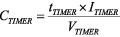
A TIMER value of less than 2 ms should be sufficient to protect the MOSFET—and greater than 0.9 ms to charge the load. If a conservative value of 1 ms is selected, the capacitance can be calculated as follows:
where ITIMER = 60 μA and VTIMER = 1.3 V,
When using paralleled MOSFETs, the calculations for TIMER selection will not change. It is critical that the TIMER and short-circuit protection be designed with a single MOSFET in mind. The reason is that the VGSTH can differ significantly among a population of MOSFETs, so a single MOSFET may be required to handle a large proportion of current during regulation.
Hot-Swap Design Complete
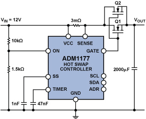
The hot-swap design with paralleled MOSFETs can be seen in Figure 7 with the correct component values. The ADM1177 hot-swap controller performs additional functions. It has an integrated on-chip ADC that can be used to translate the supply voltage and load current into digital data—which can be read out through the I2C bus, providing a fully integrated current- and voltage-monitoring function.