文章转自ADI官网,版权归属原作者一切
The universal serial bus (USB) has become a dominant interface to fulfill the ever increasing needs for rapid data transfer between end devices—for example, downloading and uploading data between PCs and portable devices such as cell phones, digital cameras, and personal media players.
CMOS switches can be used for connecting and routing data lines in USB systems. By selecting suitable switches, designers can significantly shorten design cycles by enhancing existing designs rather than developing new ones. In this article, we describe the USB, then go on to explore the crucial role of switches in improving performance in applications such as portable media players, cell phones, and wireless pen drives. We also show how key parameters of the switches affect the overall system design and discuss basic design challenges, such as the trade-offs between meeting bandwidth requirements and minimizing signal reflections. Additionally, we suggest how to maximize the opening in eye diagrams by careful board layout.
What Is USB and Why Has It Become So Popular?
USB has become the most popular standard for PC-to-peripheral communication in the world. Keyboards, printers, data-storage devices, and mobile phones are among the many peripherals that can be connected to a PC, employing the USB standard. Devices that previously used serial ports and parallel ports are migrating to USB, while designers of devices such as hard drives and digital cameras are often choosing USB over other standards, such as FireWire or serial-port communication. Connectivity to mobile phones, MP3 players, and game consoles is another recent development.
USB’s main attraction is the ability to plug and play. The device is plugged into the PC, recognized by the PC; then, after the first installation of appropriate software, the device will always be recognized by the host PC—a user-friendly handshake.
The USB Implementers Forum, Inc., an industry-standard-generating body sponsored by leading companies from the computer and electronics industry, lays down the standards for USB. Device designs can receive USB certification—and use the USB symbol on a product, but only after passing very strict software and hardware tests. This ensures that all USB-certified devices, whether PC or peripheral, will function correctly when interconnected, from the standpoints of both software and hardware. The standard ensures that all certified software routines, connectors, cables, signal drivers, and receivers comply, ensuring interconnnectability (Figure 1a).

USB is based on a serial master-slave architecture. In general, the PC is the master, known as the host (Figure 1b); it controls the transaction. The slave, known as the peripheral, tells the host its bandwidth requirement, and then a data transaction is initiated. A complete sequence of normal USB events includes these steps:
- Peripheral plugged into host (initiating USB event)
- Handshaking (peripheral identified, bandwidth allocated)
- Bulk data transfer (e.g., to printer), or peripheral polled (mouse)
- Peripheral disabled by host
- Peripheral disconnected

The hardware used in a USB system transmits data using a 2-wire (plus ground) differential bidirectional system. The data lines, D+ and D–, transmit the data as shown in Figure 2. Data can only be transmitted in one direction, so in one instance the host transmits while the peripheral receives, and then the peripheral transmits while the host receives. The USB standard also includes a 5-V power line. Generally used to power downstream devices, it obviates the need for batteries in low-power devices such as USB pen drives, webcams, and keyboards.

How Do USB 1.1 and USB 2.0 Compare?
The USB standard specifies three data rates: Low-Speed (1.5 Mbps), Full-Speed (12 Mbps), and Hi-Speed (480 Mbps). USB 1.1 devices have ±3.3-V signal levels and can operate at low- and full speeds. USB 2.0 devices have ±400-mV signal levels and can operate at low-, full-, and high speeds.
Table I. Comparison of USB 1.1 and USB 2.0
| USB 1.1 | USB 2.0 | |
| Symbol |
 |
 |
| Nomenclature | Low-/Full-Speed | Low-/Full-/Hi-Speed |
| Bit Rate (Mbps) | 1.5/12 | 1.5/12/480 |
| Single-Ended Amplitude | 0 V to 3.3 V | 0 V to 400 mV |
What Is USB On-The-Go (USB OTG)?
Many consumer products—such as cell phones and digital cameras, that connect to the PC as a USB peripheral—can also be connected to other USB devices. Since, in these circumstances, the PC cannot be the host, one of the peripherals needs to take on the responsibility. USB OTG defines a dual-role device, which can act as either a host or a peripheral—and can use the same connector for both PCs and other portable devices.
By enabling basic functions between digital devices, USB OTG makes these PC peripherals more capable, hence more valuable to consumers and corporate users. USB OTG devices will, of course, connect to PCs, as they comply with the USB 2.0 specification. In addition, they will have limited host capability to allow them to connect to a targeted set of other USB peripherals. When two dual-role devices get connected together via a cable, the cable sets a default host and default peripheral. If the application requires that the roles be reversed, the Host Negotiation Protocol (HNP) provides a handshake to perform that function, a reversal completely invisible to the user.
What Are the Switch Requirements for USB 1.1/USB 2.0?
The USB data lines, D+ and D–, can be connected and routed by internal CMOS switches. In the example of Figure 3, a switch is connected in series with each data line. Additional switch capacity is available by using multiplexers. Low-, Full-, and Hi-Speed USB use a 45-ohm system; the driver has a source impedance of 45 ohms, and the receiver has a termination of 45 ohms to ground. All USB cables and tracks should have a single-ended impedance of 45 ohms to preserve signal integrity. We will discuss transmission-line impedance and board layout later

USB standards call for stringent tests to ensure that signals are handled in conformance with their requirements. One of the key tests is an “eye” diagram. This is an intuitive visual test, which can tell a lot about the signal’s quality. An eye diagram is generated by probing a randomly varying digital signal, plotting it vs. sweeps of one or more cycles, and setting the scope for long persistence. The result is that all possible bit permutations are overlaid on a single view, showing the range of deviations from an ideal “eye” pattern in amplitude, phase, and rise- and fall times. Hence any bit patterns that could cause problems may be seen on the plot.
Figure 4, taken from the USB-IF spec, shows the setup used to establish the eye diagram. The “SQiDD” (signal quality drop/droop) test board, which the USB-IF distributes, functions as a host; and the mouse (the device under test) is plugged into this board. The signals D+ and D– are probed, and then overlaid on the scope, generating the eye diagram. The eye opening is then compared with a mask of the required shape to allow the viewer to see if the signal quality complies with the USB standard.

In testing the suitability of CMOS switches for use in USB products, they cannot be tested by temselves as USB devices, since they are used within the device in the signal path. Therefore, a data generator could be used to generate the required signal, and this signal, passing through the switch, is terminated at the scope. The scope is triggered using an external clock, which is synchronized with the random digital signal. This will result in an eye diagram of the CMOS switch.
For example, a set of typical eye diagrams is shown in Figure 5, generated at USB Hi-Speed data rates (480 Mbps) and signal levels (0 to 400 mV). They compare the performance of ADG774A (bandwidth >500 MHz) and ADG736 (200-MHz bandwidth) CMOS switches, passing the same signals. Included in the plot is a USB-IF mask (red hexagon). According to the USB spec, if the signal crosses the boundaries of the mask, the device fails on signal integrity.

The illustration shows that the ADG774A complies with the mask, displaying little ripple, even at these high data rates. The ADG736, however, with its higher capacitance and lower bandwidth, has slowed down the edges, thereby causing the signal to cross the mask on the left side—a clear violation, which disqualifies it from being used to pass Hi-Speed USB signals. Other noteworthy information is the lack of horizontal symmetry in the ADG736 eye, whereas the ADG774A is quite symmetrical, even at this high data rate. Both switches exhibit good symmetry vertically, however, which would indicate good matching of the two channels on both devices. Channel matching is a big concern when selecting a switch for USB applications. In a differential system, the D– signal must be the exact inverse of the D+ signal. Mismatches in cable length, capacitance, and resistance between the D+ and D– lines can cause serious skew in the eye, manifested as vertical asymmetry. The point where the signals cross (the crossover point) should be centered on ground. Jitter is also critical to USB qualification. The thicker the edges, the worse the jitter—not a problem with these CMOS switches. Actually, the jitter seen was also visible with the switch removed, suggesting that the jitter exists in the system.
Figure 6 is a typical plot for an ADG787, using a USB Full-Speed signal (0 V to 3 V, 12 Mbps) in a setup similar to the one used for the above plots. The mask shown is taken from the USB-IF spec for USB Full Speed. The signal used had a rise- and fall time of six nanoseconds. As can be seen, the signal is free from the faults discussed above. No mask violation, good jitter, good crossover and symmetry, and little rippling can be observed. These plots demonstrate the value of an eye diagram, in that at a glance we can conclude that this ADG787 can easily pass a Full-Speed USB signal.

How to Choose a CMOS Switch for USB Applications
We now illustrate the specific requirements of a switch and how they affect the signal. This section will consider the correlation between switch specifications and overall system signal integrity.
Switch requirements for both standards would call for as low an on resistance as possible, combined with low capacitance. The characteristics of the two switches need to be matched as accurately as possible to keep the data-line symmetry.
On Resistance
In a 45-ohm system, an on resistance of greater than 5 ohms is undesirable, as a 5-ohm on resistance will add to the source impedance, making it 50 ohms. In order for the receiver to receive a 3-V signal, the 45-ohm source transmits a 6-V signal, which is ideally halved by the divider formed by the 45-ohm source and the termination impedance. This is illustrated in Figure 7, which shows the switch as a resistance in series with the driver. With 5 ohms in series, the receiver sees a 50-ohm source and 45 ohms to ground.

The equations compare performance of an ideal switch with one having 5 ohms of series resistance. A significant loss (>5%) is introduced by the switch. Therefore low Ron is critical.
 |
 |
The source-to-drain resistance of a CMOS switch varies with both the supply voltage and the bias voltage, as illustrated in the Ron plot for an ADG787 switch. As the voltage on the source is varied, the resistance measured from source to drain changes.

If the resistance of the switch varies, with either bias voltage, temperature, or supply, the amplitude seen by the receiver will also vary, as can be seen for a varying Ron (i.e., Ron + Δ Ron).

Ron flatness is also vital to ensuring that the rise- and fall times of the switch are as close as possible. If Ron varied significantly with bias, the rising and falling edges would see different impedances at different stages in their transition. Differences here would be seen as poor crossover in the eye diagram.
Therefore, Ron variability with supply voltage, temperature, and bias are big considerations when designing a switch for use in USB products. Variability of Ron over supply tolerances and temperature would be seen on the eye diagram as jitter. As a rule, lower Ron means lower flatness and distortion, as can be seen by comparing Figure 9 (ADG836) with Figure 8. The ADG836, which is a dual-SPDT switch fabricated on a 0.35-µm geometry, has Ron of about 0.5 ohms and 0.05-ohm flatness, compared with 2 ohms and 0.25-ohm flatness for the ADG787. Keeping Ron low is the key to keeping Ron flatness low.

Channels should be matched as closely as possible when designing, to ensure Ron and ΔRon are the same for the two switch channels passing the differential signals. An eye diagram would indicate poor matching of on resistances.
Capacitance
Capacitance of CMOS switches in the on state increases with size of the switch. However, since low on resistance is achieved by increasing the size of the switch, there is a direct trade-off between Ron and capacitance. This capacitance, which dictates the bandwidth of the switch, becomes more critical for Hi-Speed USB signals, where switch capacitance greater than 10 pF can significantly degrade the signal. The high capacitance slows the edges down, causing the eye to cross the mask. This was seen in the comparison of the ADG736 and the ADG774A USB Hi-Speed eye diagram of Figure 5. The ADG736 has a bandwidth of 200 MHz. The ADG774A has a much lower capacitance with a bandwidth of 400 MHz. A –3-dB switch bandwidth of greater than 6 MHz (12 Mbps) is required for USB Full Speed, with 240 MHz (480 Mbps) required for Hi-Speed USB. The layout engineer needs to ensure very close similarity of switch layouts to maintain symmetry capacitively.
Propagation Delay
By itself, a CMOS switch in the closed state adds negligible delay to a digital signal passing through it. The switch introduces no buffers in the path, and it can be modeled as a series resistance. The only real delay added by the switch is the time taken by the signal to get to the die, and out again. This value can be measured in picoseconds.
Supplies
For Low- and Full-Speed USB, the signal amplitude is 3.3 V ±10%. Therefore 3.6 V is the minimum supply allowable. The amplitude of the Hi-Speed signal is 400 mV ± 10%, which can easily be passed by a switch on a 3.3-V supply. It is possible for the CMOS switch to be powered using the USB cable’s 5-V supply line. When passing Full-Speed signals (3 V, 12 Mbps), a full signal range is desirable.
Switch Protection
The USB spec states that the data lines of a USB device must be able to withstand being shorted to the 5-V supply line for a period of 24 hours. This has implications for using 3.3-V (0.35-µm geometry) switches in order to obtain the required Ron and capacitance. It also has implications for portable devices such as handsets, which use a 3.3-V supply.
Figure 10 shows a 0.35-µm switch being supplied by a 3.3 V regulator, at the input to a USB transceiver. One channel is shown for simplicity. This is a typical circuit using a 0.35-µm-geometry switch in a USB application.

Figure 11 introduces a short (in red) from the 5-V supply to the data line. This could happen if the device were plugged into a faulty port.

The short circuit forward-biases the ESD (electrostatic-discharge-protection) diode to VDD, which means that 500 mA could flow continuously through the ESD diode—a circumstance potentially very damaging to the CMOS switch, which would not be likely to survive over 24 hours. This is a limitation in implementing 0.35-µm parts. In systems that require this USB condition to be met, and a 3-V switch was to be used, the designer would need to provide adequate protection to prevent this failure mechanism. The easiest way of doing this is using a resistor to limit the current flow. However, the most common solution is to avoid this altogether by using a switch powered from 5-V supplies.
Consumer Applications
Having shown the basic ways in which switches are used in USB applications, we now survey some specific areas of application and discuss the ways they make use of switches. It will be noted that many of them have common topologies.
Portable Media Players (PMPs)
PMPs are rapidly becoming a must-have gadget throughout Asia; it is predicted that they will soon replace the MP3 market. PMPs can record directly from a TV, VCR, DVD player, cable box, or a satellite receiver, and can store up to 120 hours of video, 300,000 pictures, 16,500 songs or 30 GB of data. A portable device that can store this amount of data must have a fast, easy-to-use interface. The interface of choice, usually USB Hi Speed, is one that can be used with a USB camera, USB card reader, or USB hard drives.
Consumer demand for this type of product also dictates a slim, portable device, so traditional bulky headphone connectors could not even be considered. Instead, the headphone connector is replaced by a mini USB connector, which is shared by the USB data stream and audio outputs.
As shown in Figure 12, a switch is typically needed to isolate the USB signal from the analog audio output. This minimizes reflections by isolating the audio signals from the connector D– and D+ pins when in data mode. Reflections during fast signal logic state transitions can potentially cause higher bit-error rates and violate the 500-ppm accuracy requirement of the USB High-Speed connection.
For applications of this kind, switches with wide bandwidth and good on-resistance matching help minimize USB signal-edge distortion, while in audio mode (output connected to a headphone), low on resistance (about 2.5 ohms), and low total harmonic distortion (about 0.1%) are critical to minimize audio distortion.

Handsets/Cell Phones
As handsets acquire additional features, the challenges to a designer also increase. Many of the currently available handsets have cable connections to link to a PC. These connections are used to transfer data, such as emails, calendar, phone book, alarm clock, voice memos, and calculators. If the handset has an integrated camera, the ability to download pictures is also an attractive feature.
So, a handset may have many features that generate a need for USB-compatible switches. One of the most common requirements is in switching between different data standards, for example, between UART and USB. Handset manufacturers like to retain the capability of offering a choice of data-transmission standards to their customers, but they cannot afford the area needed for a separate connector for each interface. The easiest solution is to multiplex a number of pins on a common connector. An example of this is shown in Figure 13.

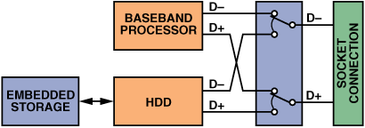
Increasing resolutions of LCD panel displays and cameras in high-end phone designs generate a requirement for larger storage devices, such as embedded hard drives or external, reduced-size memory cards. Most cell phones use standalone hard-drive controllers with a USB interface to communicate with a PC host. When a full-speed I/O port for the baseband processor is also used for synchronizing address books or other data, sharing a single USB port becomes a challenge. The design is simplified by multiplexing the phone’s USB connection, as shown in the example of Figure 14.
For both functions in a handset as described above, the specifications that need to be considered by the designer are:
- does it meet the bandwidth requirements of the chosen USB standard?
- on-resistance matching and/or matched propagation delays
- low on-resistance flatness/minimal additive jitter
- power and package size.
A further function in a handset is port/bus isolation. This function, not limited to handsets, is also used in other portable designs such as digital still cameras (DSC), PMPs, and pen drives.
Switches are commonly used to protect internal ASICs that could be interfered with by external noise. Of greater importance: for high-end portable design with USB OTG interfaces, isolation between the USB PHY (USB physical layer transceivers) and the external world can further reduce the potential risk of triggering false session-request-protocol (SRP) pulses between dual-role devices—such as two cell phones. The specification of choice for a switch in this application is off-isolation, needed when the switch is open and the USB port is not in use (Figure 15). On the other hand, when the USB bus is activated, wide switch bandwidth is needed for minimal deterministic jitter. Many Analog Devices switches are suitable for this application; the tables at the end of this article are a compact source of useful information.

Wireless Pen Drives and Wireless Adaptors
USB flash drives (pen drives) have become valuable tools for data sharing in both office and home applications because of their mobility, wireless capability, and scalable memory size. Another popular device is the USB wireless adapter; by simply plugging it into your PC, you can connect to the Internet wirelessly without the need for a Centrino™ chip, for example. Wireless USB adapters with memory storage capacity offer a convenient way for business travelers to switch between wireless Internet functions and storage and retrieval functions.
Most storage devices such as hard-disk drives or compact flash memory controllers have Hi-Speed USB interfaces, which are not integrated into a wireless LAN PHY. A USB-compatible switch can easily solve this design challenge by switching between flash memory storage and wireless functions (Figure 16). Low power consumption is desirable, since most of the power consumed by wireless USB adapters comes from the bus of the host application. Small and thin packaging is critical for such applications with very limited PCB space available inside the pen drives.

Personal Computers
The PC is at the hub of most USB systems. In all but USB OTG systems, the PC acts as the host of the system. The many traditional USB 1.1 peripherals, such as handsets, digital still cameras, modems, keyboards, mice, some CD-ROM drives, tape and floppy drives, digital scanners, and specialty printers—all interconnect with the PC. USB 2.0 Hi Speed now accommodates a whole new generation of peripherals, including MPEG-2 video-based products, data gloves, and digitizers. USB has become a built-in feature of most PC chipsets, as well as operating-system- and other system software, without significantly affecting PC prices. By eliminating add-in cards and separate power supplies, USB can help make PC peripheral devices more affordable than they would be otherwise. In addition, USB’s hot-swap capability allows users to easily attach and detach peripherals.
As with handsets, CMOS switches can be used to expand the USB bus internally. A further function of switches is in peripheral multiplexing. Figure 17 shows a printer being shared by multiple PCs.

Board Layout Considerations
Signal routing is key to performance in USB systems. This section details recommended USB PCB signal routing. These comments are based on the system chosen by the USB-IF in order that board and cable designers could design boards that have as little effect on the USB signals as possible at all USB speeds.
As noted earlier, USB is based on a 45-ohm single-ended transmission-line system. It requires that the D+ and D– tracks have impedance to the ground plane of 45 ohms for optimum signal integrity, i.e., to help prevent reflections and signal loss for high-speed signals.
Differentially, the D+ and D– lines should have a mutual impedance of 90 ohms, that is, the impedance between D+ and D– should be 90 ohms.
An impedance calculator should be used to come up with the differential trace spacing. In the example of Figure 18, a useful spacing for 1-ounce copper was calculated to be as shown.

Continuing with the above example, and knowing the track width to be 7.5 mils (0.1905 mm), a layer stackup depth can be calculated for 45-ohm single-ended impedance. Prepreg is the dielectric, commonly Rogers material or FR4. The dielectric constant of this material is critical in calculating the depth to the ground plane. The prepreg in the example of Figure 19 has a dielectric thickness of 4.5 mils, with 1-ounce copper traces and planes.

In the stackup shown, two internal planes were used, enabling signals to be routed along the top and bottom of the four-layer board. For a two-layer board, the stackup would only include the signal tracks, prepreg, and ground plane, with the same spacings and dielectric.
The board shown in Figure 20, using the above stackup and spacings, was employed to evaluate Analog Devices CMOS switches for USB-style measurements. USB connectors were also incorporated on the board.

With rise- and fall-time edges of Hi-Speed USB as fast as 500 picoseconds, an impedance mismatch can result in transmission-line reflections. In order to avoid reflections, a switch should ideally be placed as close as possible to the USB driver output. The switch would then be seen as a lumped load at the driver output, and there would be minimal signal reflections. In addition, this placement helps improve EMI performance.
The difference between the trace lengths carrying the differential signals should be minimized to optimize the skew between channels; this helps to decrease the deterministic jitter (nonrandom, repeatable, or predictable jitter). For best signal integrity, minimal trace length between the USB driver and the connector is recommended. A lower bandwidth results in edge roll-off of the USB signals and may contribute to increased phase jitter and noise.
In addition to the natural decoupling capacitor between the power and ground planes inherent in the four-layer designs, additional paralleled decoupling capacitors (1 µF and 0.1 µF) should be attached close to the Vdd pin of the switch.
If the application requires higher ESD performance than is already available in the switch (for example, ADG787 has 2-kV HBM), you may add external ESD devices to the bus. However, it is recommended that the input/output capacitance of external ESD devices be less than 1 pF, and that they be placed close to the USB connector port to minimize bus loading.
For minimal static power consumption, the switch-control signal should swing as closely as possible between 0 V and Vdd.
Finally, if the USB controller’s output-signal eye diagram has little passing margin or already fails the USB eye mask requirement, adding a switch will not result in successful eye compliance. To improve the eye, the output drive of the controller should be increased, or board-layout issues should be resolved, before the switch is incorporated.
Conclusion
With the increasing prevalence of USB functions in both portable and hand-held applications, high-quality switches, using ultralow power, are playing a key role. Analog Devices switches, with their small-footprint packaging, allow designers to add high-speed functionality to existing full-speed platforms at low cost and shorten the time-to-market for their applications. These factors, driven by the consumer demand for continual innovation, accelerated design, and reduced manufacturing cycles, are critical considerations for designers.
Selection Table for 12 Mbps
| Generic | Configuration | Supply | Package | Specifications |
| ADG711/ADG712/ADG713 |
Quad SPST |
5 V |
16-lead TSSOP/SOIC |
2-ohm Ron, >200 MHz B/W |
| ADG781/ADG782/ADG783 |
Quad SPST |
5 V |
20-lead LFCSP |
2-ohm Ron, >200 MHz B/W |
| ADG721/ADG722 |
Dual SPST |
5 V |
8-lead MSOP |
2-ohm Ron, >200 MHz B/W |
| ADG736 |
Dual SPDT | 5 V |
10-lead MSOP |
2-ohm Ron, >200 MHz B/W |
| ADG774 |
Quad SPDT |
5 V |
16-lead SOIC |
2-ohm Ron, >200 MHz B/W |
| ADG784 |
Quad SPDT |
5 V | 20-lead LFCSP |
2-ohm Ron, >200 MHz B/W |
| ADG788 |
Quad SPDT |
5 V |
20-lead LFCSP |
2-ohm Ron, >200 MHz B/W |
| ADG821/ADG822 |
Dual SPST |
5 V |
8-lead MSOP |
<1-ohm Ron, 24 MHz B/W |
| ADG709 |
Dual 4:1 Mux |
5 V |
16-lead TSSOP |
3-ohm Ron, 100 MHz B/W |
| ADG729 |
Dual 4:1 Mux |
5 V |
16-lead TSSOP |
3-ohm Ron, 100 MHz B/W, I2C® |
| ADG739 |
Dual 4:1 Mux |
5 V |
16-lead TSSOP |
3-ohm Ron, 100 MHz B/W, SPI® |
| ADG759 |
Dual 4:1 Mux |
5 V |
20-lead LFCSP |
3-ohm Ron, 100 MHz B/W |
Selection Table for 480 Mbps
| Generic | Configuration | Supply | Package | Specifications |
| ADG3241 | SPST | 3.3 V | SC70, SOT-66 | 2-ohm Ron, >480 MHz B/W |
| ADG3242 | 2 × SPST | 3.3 V | SOT-23 | 2-ohm Ron, >480 MHz B/W |
| ADG3243 | 2 × SPS | 3.3 V | SOT-23 | 2-ohm Ron, >480 MHz B/W |
| ADG3245 | 8 × SPST | 3.3 V | TSSOP, LFCSP | 2-ohm Ron, >480 MHz B/W |
| ADG3246 | 10 × SPST | 3.3 V | TSSOP, LFCSP | 2-ohm Ron, >480 MHz B/W |
| ADG3247 | 16 × SPST | 3.3 V | TSSOP, LFCSP | 2-ohm Ron, >480 MHz B/W |
| ADG3248 | SPDT | 3.3 V | SC70 | 2-ohm Ron, >480 MHz B/W |
| ADG3249 | SPDT | 3.3 V | SOT-23 | <1-ohm Ron, >480 MHz B/W |
| ADG774A | 4 × SPDT | 5 V | QSOP, LFCSP | 2.2-ohm Ron, >400 MHz B/W |
| ADG3257 | 4 × SPDT | 5 V | QSOP | 2.2-ohm Ron, >400 MHz B/W |