文章转自ADI官网,版权归属原作者一切
Charged device model (CDM) ESD is considered to be the primary real-world ESD model for representing ESD charging and rapid discharge and is the best representation of what can occur in automated handling equipment used in manufacturing and the assembly of integrated circuits (ICs) today. It is well known that the largest cause by far of ESD damage to an IC during device handling in a manufacturing environment is from charged device events.1
Charged Device Model Roadmap
With the ever increasing demand for higher speed IOs in ICs and the need for packing more functionality into a single package driving larger package sizes, efforts to maintain the recommended target CDM levels as discussed in JEP1572, 3 will be a challenge. It should also be noted that while technology scaling may not have a direct impact on target levels (at least down to 14 nm), the introduction of improved transistor performance in these advanced technologies can also enable higher IO performance (transfer rates), which can make achieving current target levels difficult for the IO designer as well. As a result of the inconsistent charging resistors between different testers, looking at published, ESD Association (ESDA) roadmaps out through the year 20204 suggests that CDM target levels will need to be reduced again, as shown in Figure 1.

While a quick look at Figure 1 would not suggest a significant change in the range of CDM target levels, a further look at data supplied by the ESDA and shown in Figure 2 shows that there is expected to be a significant change in the distribution of CDM ESD target levels.

Why is this change important to discuss? It points out the need for a consistent way to test CDM across the electronics industry without some of the inconsistencies created by having multiple test standards. It is more important now than ever to ensure manufacturing is properly prepared for the CDM roadmap discussed by the ESDA. One critical piece of that preparation is ensuring that manufacturing receives consistent data from each semiconductor manufacturer on the CDM robustness level of their devices. The need for a harmonized CDM standard has never been greater. This, coupled with continued technology advancements, may also drive higher IO performance. This need for higher IO performance (and its need for reduced pin capacitance) may leave an IC designer with no other option other than lowering the target levels, which in turn demands a more precise measurement (which is addressed within ANSI/ESDA/JEDEC JS-002).
A New Joint Standard
Prior to ANSI/ESDA/JEDEC JS-002, there were four existing standards: the legacy JEDEC (JESD22-C101),5 ESDA S5.3.1,6 AEC Q100-011,7 and EIAJ ED-4701/300-2 standards.8 ANSI/ESDA/JEDEC JS-002 (charged device model, device level)9 represents a major first push toward harmonization of these four existing standards into a single standard. While all of these methods produce valuable information, the presence of several standards is not a benefit to the industry. The different methods often produce different passing levels, and the presence of several standards requires manufacturers to support multiple test methods with no increase in meaningful information. Therefore, it is vitally important that a single measurement level of an IC’s charged device immunity is well known to ensure the CDM ESD design strategy has been implemented correctly and that the IC’s charged device immunity is matched to the level of ESD control in the manufacturing environment to which it will be exposed.
JS-002 was developed by a combined ESDA and JEDEC CDM Joint Working Group (JWG) formed in 2009 to address this issue. Additionally, the JWG wanted to make technical improvements to the field-induced CDM (FICDM) method based on lessons learned since FICDM was introduced.10 Finally, the JWG wanted to minimize disruption in the electronics industry. To reduce industry disruption, the working group decided that the joint standard should not require purchasing of totally new field induced CDM testers and pass/fail levels should be matched as close as possible to the JEDEC CDM standard. With the JEDEC standard being the most widely used CDM standard, this keeps JS-002 aligned with current manufacturing understanding of CDM.
While the JEDEC and ESDA test methods are very similar, there are a number of differences between the two standards that needed to be resolved. There are also technical issues that JS-002 seeks to address. Some of the most important issues are listed below.
Differences between the standards
- Field plate dielectric thickness
- Verification modules used to verify systems
- Oscilloscope bandwidth requirements
- Waveform verification parameters
Technical issues with standards
- Measurement bandwidth requirements too slow for CDM
- Pulse width in JEDEC’s standard is artificially wide
- Waveform and equipment geometry requirements forced hidden voltage adjustments
To address the objectives and harmonize, the following hardware and measurement choices were made. Extensive measurements were made during the five-year process of document creation in arriving at these decisions.
Hardware choices
- Use the JEDEC dielectric thickness
- Use the JEDEC coins for waveform verification
- Forbid use of ferrites in the discharge path
Measurement choices
- Require a 6 GHz minimum bandwidth oscilloscope for system verification/acceptance
- Allow the use of 1 GHz oscilloscope for routine system verification
Minimize data disruption and discuss hidden voltage adjustments
- Align target peak currents with existing JEDEC standard
- Specify test conditions matching JEDEC stress levels; for JS-002 test results, we refer to test conditions (TCs) and for JEDEC and AEC, we refer to volts
- Field plate voltage adjusted for JS-002 to provide correct peak current corresponding to the legacy JEDEC peak current requirements
Ensure full charging of large packages
- To ensure full charging of large packages, a new procedure was introduced
The next sections describe these improvements.
JS-002 Hardware Choices
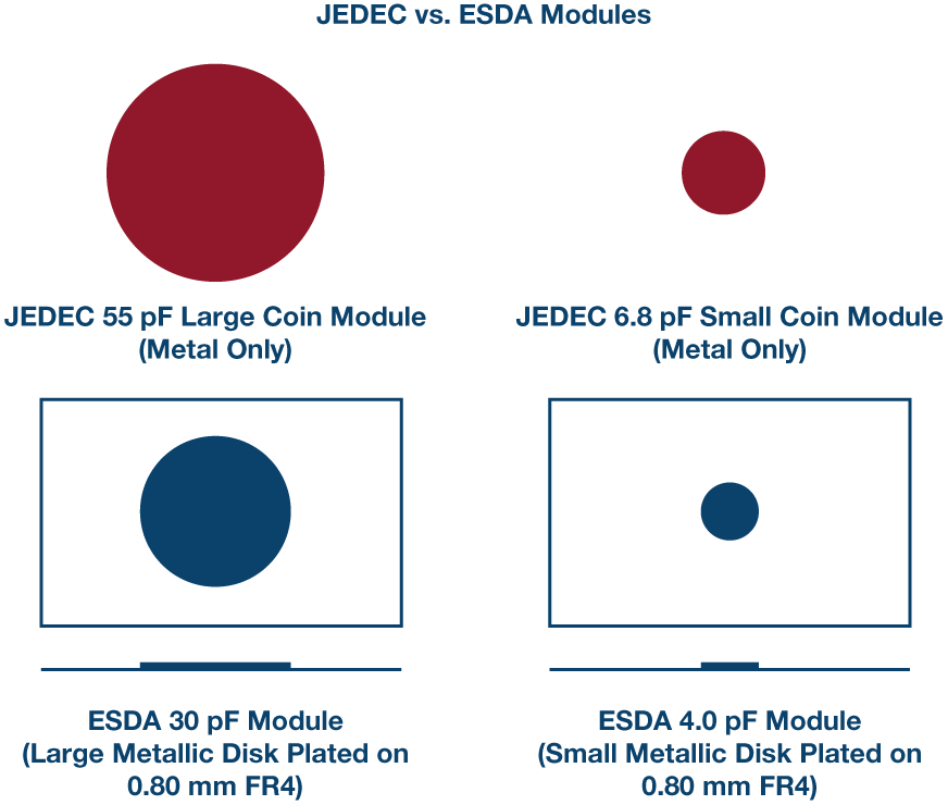
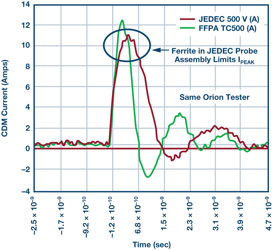
The JS-002 CDM hardware platform represents a combination of the ESDA S5.3.1 probe assembly, or test head discharge probe and the JEDEC JESD22-C101 verification module and field plate dielectric. Figure 3 shows this hardware comparison. The ESDA probe assembly was designed not to have a specific ferrite in the discharge path. FICDM tester manufacturers found that a ferrite was necessary and was added to increase the full width at half maximum (FWHH) specified minimum value of 500 ps and reduce the Ip2 (second waveform peak) to below 50% of first peak Ip1 to meet legacy JEDEC requirements. JS-002 removes this ferrite to remove this limiting factor in the discharge, resulting in a more accurate discharge waveform that eliminates the ringing seen at Ip1 with a high bandwidth oscilloscope.

Figure 4 shows the difference in the ESDA and JEDEC CDM standards verification modules. The ESDA standard has an option for two dielectric thickness options combining with its verification module (the second option being an additional (up to 130 μm) plastic film between its module and the field plate, addressing testing of devices with metal package lids). The JEDEC verification module/FR4 dielectric represents a single small/large verification module and dielectric option supported by the much larger community of JEDEC standard users.
JS-002 Measurement Choices
During its data gathering phase of the JS-002 standard development, the CDM JWG found that a higher bandwidth oscilloscope was necessary to accurately measure the CDM waveform. A 1 GHz bandwidth oscilloscope does not capture the true first peak. Figure 5 and Figure 6 illustrate this.

Routine waveform checking, such as daily or weekly checks, can still be done using a 1 GHz bandwidth oscilloscope. However, analysis across lab test sites has shown that a high bandwidth oscilloscope provides better site-to-site correlation.11 A recommendation to use the high bandwidth oscilloscope for routine and quarterly checks is included. Annual verifications or verifications after tester hardware changes or repair require the high bandwidth oscilloscope.
Tester CDM Voltage Settings
The CDM JWG also discovered that across tester platforms significant variation in the actual plate voltage setting (for example, 100 V or more at a specific voltage setting) was needed to obtain standard test waveform compliance in the previous ESDA and JEDEC standards. This was not described in any of the standards. JS-002 is unique in determining the offset or factor required to scale first peak current (and voltage represented by a test condition) to the JEDEC peak current levels. Annex G of JS-002 describes this in detail. Table 1 shows an example of verification data incorporating this feature.
| Tester—System #1 | |||||||||
| Polarity = Postive | Scope Bandwidth = 8 GHz | Factor/Offset Final Setting = 0.82 | |||||||
| Module Size | Date | %RH | Test Cond | Software Voltage | Ip AVG (A) | TR AVG | TD AVG | IP2 AVG | IP2 (% IP1) |
| Large | dd/m/yy | X% | TC 500 | 500 | 12.1 | 275 | 610 | 4.3 | 36% |
| Small | dd/m/yy | X% | TC 500 | 500 | 7.30 | 185 | 400 | 3.7 | 51% |
| Large | dd/m/yy | X% | TC 125 | 125 | 2.90 | 283 | 611 | 1.1 | 38% |
| Small | dd/m/yy | X% | TC 125 | 125 | 1.90 | 201 | 395 | 1.1 | 58% |
| Large | dd/m/yy | X% | TC 250 | 250 | 6.00 | 276 | 609 | 2.2 | 37% |
| Small | dd/m/yy | X% | TC 250 | 250 | 3.70 | 186 | 397 | 2.1 | 57% |
| Large | dd/m/yy | X% | TC 750 | 750 | 18.30 | 274 | 611 | 7.2 | 39% |
| Small | dd/m/yy | X% | TC 750 | 750 | 11.00 | 190 | 398 | 6.1 | 55% |
| Large | dd/m/yy | X% | TC 1000 | 1000 | 24.40 | 276 | 612 | 9.2 | 38% |
| Small | dd/m/yy | X% | TC 1000 | 1000 | 14.60 | 187 | 399 | 7.4 | 51% |
Ensuring Full Charging of Very Large Devices at a Set Test Condition
During the data gathering phase of the JS-002 development, another tester-dependent issue was discovered whereby some test systems were not fully charging large verification modules or devices to their set voltage before discharging. It was found that the high value field plate charging resistor (a series resistor between the charging supply and the field plate) was not consistent between test systems, affecting the delay time required for full plate voltage charging. As a result, the first peak discharge currents could vary among testers, affecting the pass/fail CDM classification especially for large devices.
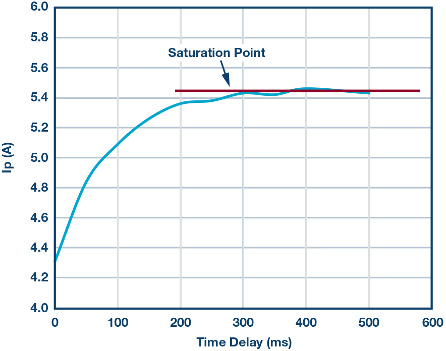
Because of this, Informative Annex H (“Determining the Appropriate Charge Delay for Full Charging of a Large Module or Device”) was written to describe a procedure for determination of the delay time needed to fully charge a device. An appropriate charge delay time is reached when a peak current saturation point (where Ip attains a basically constant value independent of longer decay time settings) is found to occur, as shown in Figure 7. Determining this delay time ensures that very large devices are fully charged to a set test condition prior to discharge.
Phase-In of JS-002 in the Electronics Industry
The JS-002 standard replaces and obsoletes the ESDA S5.3.1 CDM standard for those companies using S5.3.1 as the standard. For those previously using JESD22-C101, the JEDEC reliability test specifications document JESD47 (specifying all reliability test methods for JEDEC electronic components) was recently updated to specify JS-002 in place of JESD22-C101 (in late 2016). A phase-in period is now in effect regarding JEDEC member company transition to JS-002. Many companies, including ADI and Intel, have already transitioned to testing using JS-002 for all new products.
The International Electrotechnical Commission (IEC) recently approved and updated its CDM test standard, IS 60749-28.12 This standard incorporates JS-002 in its entirety as its specified test standard.
The Automotive Electronics Council (AEC) currently has a CDM subteam committee updating the Q100-011 (integrated circuit) and Q101-005 (passive components) automotive device CDM standard documents to incorporate JS-002, with AEC specified test use conditions. These are expected to be completed and approved by the end of 2017.
Summary
As we look at the CDM ESD roadmap provided by the ESDA, CDM target levels will continue to be lowered, driven by higher IO performance. Manufacturing awareness of device level CDM ESD withstand voltage is more critical than ever and cannot be accurately communicated by inconsistent product CDM results coming from different CDM ESD standards. ANSI/ESDA/JEDEC JS-002 has the opportunity to be the first true industry-wide CDM test standard. The removal of inductance in the CDM test head discharge path significantly improves the quality of the discharge waveform. The introductions of a high bandwidth oscilloscope for verification, the increase to five test condition waveform verification levels, and an assurance of the correct charging delay time all significantly reduce cross-lab variation in test results—improving repeatability from site to site. This is critical to ensure consistent data is supplied to manufacturing. With JS-002 acceptance across the electronics industry, the industry will be in a much better position to address the ESD control challenges ahead.
参阅电路
1. Roger J. Peirce. “The Most Common Causes of ESD Damage.” evaluation Engineering, November, 2002.
2. Industry Council on ESD Target Levels. “Industry Council White Paper 2: A Case for Lowering Component Level CDM ESD Specifications and Requirements.” EOS/ESD Association, Inc., April, 2010.
3. “JEP157: Recommended ESD-CDM Target Levels.” JEDEC, October, 2009.
4. EOS/ESD Association Roadmap.
5. “JESD22-C101F: Field-Induced Charged-Device Model Test Method for Electrostatic Discharge Withstand Thresholds of Microelectronic Components.” JEDEC, October, 2013.
6. “ANSI/ESD S5.3.1: Electrostatic Discharge Sensitivity Testing—Charged Device Model (CDM) Component Level.” EOS/ESD Association, December 2009.
7. “AEC-Q100-011: Charged Device Model (CDM) Electrostatic Discharge Test.” Automotive Electronics Council, July 2012.
8. “EIAJ ED-4701/300-2, Test Method 305: Charged Device Model Electrostatic Discharge (CDM-ESD).” Japan Electronics and Information Technology Industries Association, June, 2004.
9. “ANSI/ESDA/JEDEC JS-002-2014: Charged Device Model (CDM) Device Level.” EOS/ESD Association, April, 2015.
10. Alan W. Righter, Terry Welsher, and Marti Ferris. “Progress Towards a Joint ESDA/JEDEC CDM Standard: Methods, Experiments, and Results.” EOS/ESD Symposium, September, 2012.
11. Theo Smedes, Michal Polweski, Arjan van IJzerloo, Jean-Luc Lefebvre, and Marcel Dekker. “Pitfalls for CDM Calibration Procedures.” EOS/ESD Symposium, October, 2010.
12. “IEC IS 60749-28, Electrostatic Discharge (ESD) Sensitivity Testing–Charged Device Model (CDM)–Device Level.” International Electrotechnical Commission, 2017.