文章转自ADI官网,版权归属原作者一切
Introduction
Attaining high performance and low power consumption in MP3 players, personal media players, digital cameras, and other portable consumer applications has long challenged designers. These battery-powered systems typically employ an embedded digital signal processor (DSP) to achieve maximum processing power when handling multimedia applications and minimum power consumption when in sleep mode. Battery life is of prime importance in handheld battery-powered products, making their success directly related to the efficiency of the power system.
A key component of such systems, a step-down dc-to-dc switching regulator, efficiently derives a low supply voltage, say 1 V, from a higher-voltage supply, for example, 4.5 V. As a regulator, it must maintain a constant voltage, rapidly responding to variations in the upstream supply or the load current. We will discuss here an architecture that provides good regulation, high efficiency, and fast response.
Anatomy of a Switching Regulator
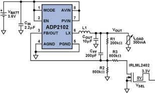
Figure 1 shows a typical application circuit using the Analog Devices ADP2102 low-duty-cycle, 3-MHz, synchronous step-down converter. It is available with a number of fixed-output and resistor-programmable voltage options. Here it is connected in a fixed-voltage configuration, producing a regulated 0.8-V output from a 5.5-V input voltage and driving a 300-mA load. A resistor-programmable application example will follow.
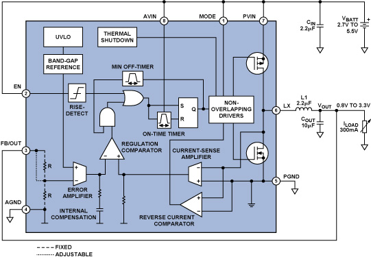
Here is a brief explanation of the circuit’s operation: A fraction of the dc output voltage is compared with an internal reference in the error amplifier, whose output is compared with the output of a current-sense amplifier to drive a one-shot that is on for a period of time that depends on the ratio VOUT/VIN. The one-shot turns on the upper gating transistor and the current in inductor L1 ramps up. When the one-shot times out, the transistor is turned off, and the current ramps down. After an interval determined by the minimum-off-timer and the minimum (“valley”) current, the one-shot is pulsed again. The on-chip one-shot timer employs input voltage feedforward for maintaining a constant frequency in the steady state.
This oscillation continues indefinitely—at approximately 3 MHz, but deviating as necessary to respond to transient line and load changes—maintaining the output voltage at the programmed value and the average inductor current at the value required by the output load.
The approach described above is relatively new. For many years, the principal approach to dc-to-dc conversion has been a constant-frequency peak-current approach, also known as trailing-edge modulation when implemented in step-down dc-to-dc converters. For a description of that approach, and an evaluation of its strengths and weaknesses vis-à-vis the constant on-time valley current-mode converter described above, see the sidebar.
The ADP2102 also includes undervoltage lockout, soft start, thermal shutdown, short-circuit protection, and ±1% feedback accuracy. This architecture allows the on-time of the main switch to go as low as, or lower than, 60 ns.
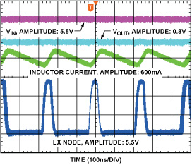
Figure 2 shows typical waveforms under various conditions. Figure 2a shows the low duty cycle that accompanies the large voltage reduction from VIN = 5.5 V to VOUT = 0.8 V at ILOAD = 600 mA. As can be seen in the plot, the minimum on-time achieved is 45 ns with a switching frequency of 3 MHz.
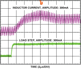
Figure 2b shows the load current and inductor current in response to a 300-mA step increase in load current.
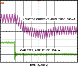
Figure 2c shows the load current and inductor current in response to a 300-mA step decrease in load current.
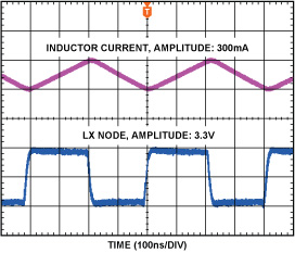
Figure 2d shows that there are no subharmonic oscillations when the part operates at a 50% duty cycle, which is a concern for parts using peak-current-mode control. This freedom from subharmonic oscillations is also the case for duty-cycle values somewhat greater or less than 50%.
Dynamic Voltage Adjustment in a DSP Application
In portable applications employing digital signal processors (DSPs), switching converters typically provide the DSP’s core voltage and I/O rails. Both supplies require high-efficiency dc-to-dc converters that are designed for battery applications. The regulator that supplies the core voltage must be able to change the voltage dynamically based on the processor’s clock speed or as directed by the software. Small total solution size is also important.
Described here are improvements in system power efficiency that can be attained in battery-powered applications by replacing a Blackfin® processor’s internal regulator with an external high-efficiency regulator. Also described is the control software for the external regulator.
Dynamic Power Management
A processor’s power dissipation is proportional to the square of the operating voltage (VCORE) and linearly proportional to the operating frequency (FSW). Thus, decreasing the frequency will lower the dynamic power dissipation linearly, while reducing the core voltage will lower it exponentially.
Changing the clock frequency—but not the supply voltage—in a power-sensitive application is useful when the DSP is simply monitoring activity or waiting for an external trigger. In high-performance battery-powered applications, however, merely changing the frequency may not save enough power. Blackfin processors, and other DSPs with advanced power-management features, allow the core voltage to be changed in tandem with frequency changes, thus seeking optimal loading of the battery for each situation.
Dynamic voltage regulation in ADSP-BF53x series Blackfin processors is typically implemented with an internal voltage controller and an external MOSFET. The advantage of this approach is that a single voltage (VDDEXT) can be applied to the DSP subsystem, while the DSP derives the necessary core voltage (VDDINT) from the MOSFET. Internal registers allow the regulated core voltage to be software-controlled in order that the MIPS, and ultimately the consumed energy, can be coordinated to achieve optimal battery life.
To fully implement this internal Blackfin regulator scheme requires an external MOSFET, a Schottky diode, a large inductor, and multiple output capacitors—a relatively expensive solution with poor efficiency that uses a relatively large PCB area. The use of the large inductors and capacitors required by the integrated regulator brings the system designer into conflict with consumer desires for portable devices to be as small as possible. Along with the relatively low efficiency of the integrated regulator controller—typically 50% to 75%—this approach is less than optimally suited for high-performance, handheld, battery-powered applications.
External Regulation
The native efficiency of the Blackfin integrated approach can be improved to 90% or more by designing in a modern dc-to-dc switching converter. The size of the external components can also be reduced when an external regulator is used.
A variety of dynamic voltage-scaling (DVS) control schemes are available, ranging from switched resistors—which in some cases can be implemented by using a DAC—to pulse-width modulation (PWM), which can achieve as fine a granularity as the internal method. Whatever scheme is used must provide the ability to change the regulation level via software control. While this regulation control method is inherent with the internal regulator approach, it must be added in external approaches.
This article describes two ways to adjust the DSP’s core voltage by using an ADP2102 synchronous dc-to-dc converter to dynamically adjust the core voltage to values from 1.2 V to 1.0 V when the processor is running at a reduced clock speed.
The ADP2102 high-speed synchronous switching converter can regulate the core voltage as low as 0.8 V when powered with a battery voltage between 2.7 V and 5.5 V. Its constant on-time, current-mode control and 3-MHz switching frequency provide excellent transient response, very high efficiency, and superior line- and load regulation. The high switching frequency allows the use of ultrasmall, multilayer inductors and ceramic capacitors. Available in a space-saving 3-mm × 3-mm LFCSP package, the ADP2102 requires only three or four external components. Functionally complete, it includes safety features such as undervoltage lockout, short-circuit protection, and thermal shutdown.
Figure 3 illustrates a circuit that implements DVS. The 3.3-V system power supply on the ADSP-BF533 EZ-KIT Lite® evaluation board powers the ADP2102 buck converter, whose output voltage is set to 1.2 V using the external resistive dividers R1 and R2. A GPIO pin from the DSP is used to select a requested core voltage. Varying the feedback resistor adjusts the core voltage from 1.2 V to 1.0 V. An N-channel MOSFET modifies the voltage divider by inserting resistor R3 in parallel with R2. The 0.25-ohm RDSon of the IRLML2402 is small compared to R3. The 3.3 V GPIO voltage is used to drive the MOSFET gate. Feedforward capacitor CFF is needed for better transient performance and improved load regulation.
The general application requirements for two-level switching are:
- DSP core voltage (VOUT1) = 1.2 V
- DSP core voltage (VOUT2) = 1.0 V
- Input voltage = 3.3 V
- Output current = 300 mA
High-value resistors are used to minimize power losses through the resistive divider. The feedforward capacitor reduces the effect of the gate-to-drain capacitance during switching. The overshoot and undershoot caused during this transition can be minimized by using smaller feedback resistors and a larger feedforward capacitor, but only at the expense of additional power dissipation.
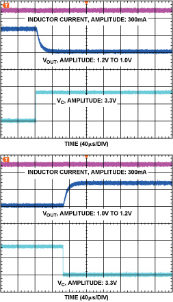
Figure 4 shows the output current, IOUT, output voltage, VOUT, and control voltage, VSEL. A low level on VSEL scales the output voltage to 1.0 V, and a high level on VSEL scales it to 1.2 V.
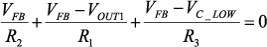
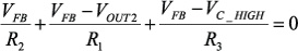
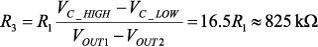
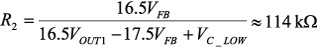
A simpler way to generate two different voltages for DVS uses a control voltage, VC, to inject current into the feedback network through an additional resistor. Adjusting the duty cycle of the control voltage varies its average dc level. A single control voltage and resistor can thus be used to adjust the output voltage. The following equations are used to calculate the values of resistors R2, R3, and the control voltage amplitude levels, VC_LOW and VC_HIGH.
 |
(1) | |
 |
(2) |
With VOUT1 = 1.2 V, VOUT2 = 1.0 V, VFB = 0.8 V, VC_LOW = 3.3 V, VC_HIGH = 0 V, and R1= 49.9 kohm, R2 and R3 can be calculated as follows
 |
(3) | |
 |
(4) |
This approach produces much smoother transitions. Any control voltage that can drive resistive loads can be used for this scheme, as opposed to the MOSFET switching approach, which can only be used with control signal sources that can drive capacitive loads. This approach can be scaled to any output voltage combinations and output load currents. Thus, DSP power dissipation can be reduced by scaling the core voltage as needed. Figure 5 shows the implementation of the above scheme. Figure 6 shows the transition between the two output voltages using this current injection method.

Further Reading
- ADP2102 data sheet. Analog Devices.
- Hariman, George and Chris Richardson. “Control Methods Solve Low Duty-Cycle Dilemmas.” Power Electronics Technology. September 2006.
- Ridley, R. B. “A new continuous-time model for current-mode control with constant frequency, constant on-time and constant off-time in CCM and DCM.” IEEE Power Electron. Spec. Conf. Record. 1990. pp. 382-389.
- Rossetti, Nazzareno and Seth R. Sanders. “Valley Design Techniques Outperform Peak Current Mode Approach for CPU Supplies.” Power Electronics Technology. July 2001.
Advantages of Constant On-time Valley-Current-Mode Control Scheme in Step-down DC-to-DC Converters
The constant-frequency peak-current control scheme regulates a high input voltage to produce a low output voltage using two loops, viz., an outer-voltage loop and an inner-current loop. Minimal phase shift exists between the control signal and the output, thus allowing simple compensation.
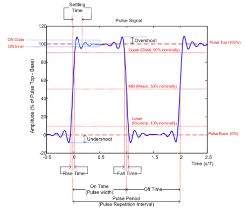
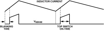
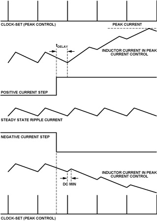
Inductor current through the NMOS main switch is typically measured by monitoring either the voltage drop across the main switch when it is on or the voltage drop across a series resistor placed between the input and the drain of the main switch. Parasitics on the switch node during inductor current-sensing cause ringing behavior in either case, so blanking time is required before the inductor current can be measured. This reduces the amount of time available for the main switch to stay on and settle during low duty-cycle operation. Figure A shows the inductor current and the current sense signal across the main switch, which consists of blanking time and on-time.
During low-duty-cycle operation, i.e., when the output is very small compared to the input, the main switch turn-on is always controlled by the internal clock and is independent of the feedback loop. Thus, a minimum on-time exists, limiting the operation at higher switching frequencies. Also, due to settling-time constraints, it is not possible to sense the current because the pulse is not wide enough. The blanking time dominates the main switch on-time, leaving very little time for current sensing. In portable applications, such as handsets and media players, output voltages of the order of 0.9 V are needed for the DSP core. A high switching frequency is desirable in order to minimize the size of the inductors and reduce the size of the overall solution; but, using this control scheme, it is difficult to generate a low-duty-cycle voltage from a higher input voltage using a high switching frequency.
A second limitation of trailing-edge modulation control is its poor transient response. Figure B shows typical waveforms in response to positive and negative changes in load current. In portable applications, fast transient response must be achieved while minimizing output capacitor size and cost. When a positive load-current step occurs at the output, the output response can be delayed by as much as one clock period. During a negative load current step, the converter forces a minimal-width high-side on-time, as determined by the speed of the current-control loop. A minimal delay response is, thus, not possible during negative load transients, and severe overshoot and undershoot transients occur. Additional capacitance must be added at the output to minimize them.
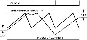
A third limitation of peak-current-control converters operating at fixed frequencies is that the instability (Figure C) at duty cycles greater than 50% allows subharmonic oscillations to occur, which cause the average output current to drop and the output current ripple to increase. For duty cycles greater than 50%, an increase in inductor current (ΔIL1) tends to increase with time, resulting in a larger increase of I2 (ΔIL2). In order to overcome this problem, slope compensation or ramp compensation is required, adding complexity to the design. Typically, an external ramp is added to the inductor current sense signal.
These problems can be overcome by using a constant on-time, valley-current-mode control scheme, known as leading-edge modulation, in which the on-time of the main switch is fixed by design; the off-time is modulated based on the valley-current-sense signal; and the switching period is adjusted to be equal to the on-time plus the off-time. This architecture facilitates high frequency operation by providing a minimum on-time for the main switch, thus allowing low voltage outputs to be easily generated from a higher input voltage.
In low-voltage dc-to-dc buck converters, the main switch is on for only 10% of the time, while the synchronous switch is on for the remaining 90% of the time. This makes it easier to sample and process the low-side switch current than the main switch current.
Instead of sensing the inductor peak current to determine the main switch current, the inductor valley is sampled during the off time of the main switch. Valley current-sensing, coupled with the constant on-time topology, reduces the loop delays, thus enabling a faster transient response.
Ray Ridley (Further Reading 3) demonstrated that the current-loop gain for constant-frequency control with an external ramp equal to the downslope of the current signal is identical to the current-loop gain of the constant-on-time system. Thus, the loop gain remains invariant with duty cycle for the constant on-time control, guaranteeing stability under all conditions. In contrast, in constant-frequency peak-current control, the loop gain increases with duty cycle and can lead to instability if insufficient external ramp time is used.
Constant on-time, variable off-time converters overcome the instability problem associated with fixed-frequency operation for duty cycles above 50% without the need for slope compensation. If the load current increases, the disturbance before the start of the cycle and at the end of cycle remains the same, and, hence, the converter remains stable regardless of the duty cycle. The absence of a fixed clock for this architecture makes the slope compensation redundant.
One of the significant benefits of constant on-time, valley-current control is the ability to limit the short-circuit current in buck converters. When the output of the buck converter short circuits and the high-side switch is on, the output voltage goes to zero and the voltage across the inductor equals VIN. The inductor current rises quickly for the duration of tON. The inductor discharge time, tOFF, increases because it is determined by VOUT/L, where VOUT is effectively a short circuit. The high-side switch doesn’t turn on again until the current has dropped to the required valley-current limit. Thus, under short-circuit conditions, this control scheme can only deliver a fixed maximum current.