文章转自ADI官网,版权归属原作者一切
[Editor’s Note: In 1993, the author presented a paper (93-070) at the ISA’s 39th International Instrumentation Conference. The interference problem he described then is even more pervasive now—15 years later—with the explosion in the applications of both RF technologies and low-frequency precision differential measurement. Because of substantial interest in the topic—as evidenced by articles in Analog Dialogue (1993, 2003) and elsewhere—the author has provided this revised and updated version of his original presentation, received February 13, 2008.]
Abstract
High frequency common mode (HFCM) is an everywhere existing condition. As long as there are working people around, there is a generator of high frequency trash. Its presence may be recognized by the mysterious errors it generates in instruments. The accuracy of many instruments including amplifiers, DVMs, and other data system components are frequently affected by the presence of high-frequency common-mode input signals. The offset errors caused by it are frequently blamed on thermally generated offsets that almost never exist. Even transducers and their excitation supplies are subject to this error source.
The Symptoms of a Problem?
Have you ever experienced a millivolt output level transducer (sensor) that seems to have excessive drift or noise? Then after replacement with another unit, the problem still exists. Perhaps the problem is not drift in the transducer? A frequently falsely identified culprit is thermally generated offsets in cable connectors or other wiring connections. A test was conducted with a several hundred foot cable run with a half dozen intermediate connectors of various manufacturers. All wire was soft copper and the connectors all were soldered brass with gold plated mating surfaces. Various connectors and portions of the cable run were exposed to temperatures as high as 150°F over a period of many hours. The sensor cable was terminated in a single constantan strain gage that was exposed to the highest temperature. During the test, the maximum peak-to-peak voltage excursion at the instrument end of the loop was 3 μV. So much for significant, thermally caused offset errors! But noise? Some are fortunate and the noise at the data amplifier output is identifiable as the talk of a cell phone or the radio station across the way. This is then the necessary clue that the amplifier is somehow sensitive to the radio frequencies that are at the amplifier input. Most are not as fortunate, however. They only experience zero offsets and they re-zero the channel and go ahead to acquire data. The data must be OK . . . After all, the sensor output was zero at the beginning of the test … They are not aware of the offset’s cause or the fact that almost without fail, the offset will change sporadically during their test to a new, significantly different offset value during the data acquisition period.
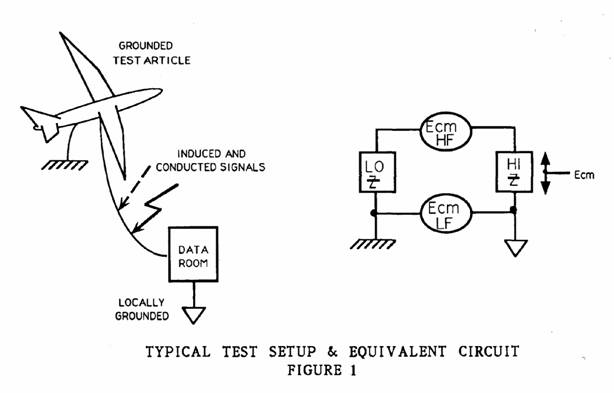
Many test situations as shown in Figure 1 have the data amplifier separated from the sensor by tens to many hundreds of feet. Whether or not the sensor is directly connected to ground at the remote location does not really matter. At high frequencies, the sensor case, its mounting surface and the sensor circuit all have enough capacitance to each other to present a ground return path. Thus, a loop antenna is formed. The high-frequency voltages developed by fields created by computers, radio stations and a myriad of other sources appear across the highest impedance of the loop. This is, almost without exception, between the amplifier input terminals and the amplifier’s ground reference. As a result, the amplifier input circuit is exposed to signals which drive it far beyond its slewing capability. This results in an offset which appears as an additional signal or, in simple terms, an offset error that is continually changing.
But, I don’t have such problems! (or do I?)
If you’d like a free lunch, courtesy of a doubting compatriot, get him (her) to bet one based on the assumption that they don’t have such problems. Then, here’s how to prove that there really is a serious problem lurking in the shadows. As shown in Figure 2, first disconnect the sensor cable and short the data amplifier input terminals. Then with the shortest wire possible, connect these shorted input terminals and the guard terminal to the amplifier’s circuit common. Observe the amplifier’s output voltage. Then replace the connection to the amplifier’s circuit common with a connection to the normally connected sensor cable conductors. If there’s a difference observed in the amplifier’s output voltage, you have observed the error caused by the different common-mode voltage at the amplifier input. After all, you did have zero (shorted) normal-mode signal in both cases. If you would like to evaluate this mysterious common-mode signal, obtain an oscilloscope with megahertz capability. Connect its common to the data system common, and its signal input terminal to the shorted sensor leads and observe the oscilloscope display. In every case when this was tried in various test laboratories of a large aerospace manufacturer, the oscilloscope showed an envelope of several hundreds of millivolts containing frequencies from power line up to many megahertz.
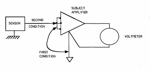
Figure 2
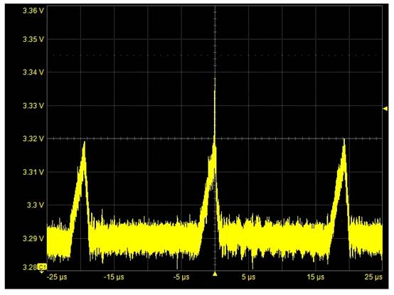
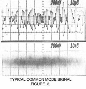
As an example, the voltage shown in Figure 3 was observed between the instrument grounds of a large laboratory data system and a laboratory about 100 feet distant. In this case, there is essentially no energy at low frequencies and significant components at frequencies in excess of a megahertz. Unacceptable offsets were even experienced when the signal source, a traceable calibration supply and the unprotected input amplifiers to be calibrated were in the same relay rack cabinet. Yes, there was a computer in a nearby cabinet.
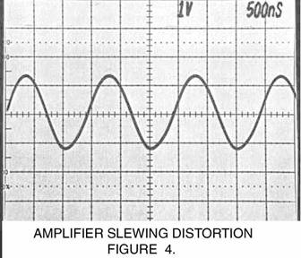
What does “unprotected input amplifier” mean? It means an amplifier which does not have any high-frequency common-mode filtering at its input. If exposed, it will most likely reach its slew limit, and since the positive-going and negative-going limits are never exactly the same, the result will be offset errors. Normal mode slew limiting can also occur with the same result, but that is usually easier to foresee. It can however be a real-life error contributor. If the amplifier is not to have slew limit caused problems, it must not be exposed to any signals, common or normal mode, which will cause it to be driven into this condition. Figure 4 shows such slewing induced distortion at about 270 degrees. This resulted in an amplifier output offset error of 3% of full scale.
The Problem
It is unusual to find a market place amplifier that does include enough protection to be unaffected in the electromagnetically unsanitary world with its undesirable high frequency common-mode signals. Probably most misleading to the inexperienced user is the marketer of integrated circuit instrumentation amplifiers. These products are very attractive to the unwary user because of the low price, good specifications and apparent ease of application. The data sheet tells about how well the amplifier works within the typical operating parameters, but fails to tell you how to stay within them under normal testing environments. Either normal or common-mode spikes that are easily generated can exceed these limits, sometimes destructively, as the device does by design have a very high input impedance. Also unfortunately, the manufacturer’s specification sheets rarely include common-mode performance above a hundred hertz or so. Exceeding this unstated limit will result in offsets and resultant data error generation.
The relationship of dc offset to high frequency common mode can not be expressed as common-mode rejection ratio, CMRR on the data sheet, since the two parameters are not coherent. If high-frequency CMRR is given, it is the relationship of output to input at that frequency. Not many instrumentation amplifier output stages will pass megahertz data under any circumstances and hence have excellent high-frequency CMRR. Specsmanship wins again!
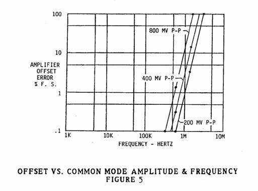
With the exception of a very few manufacturers’ products, most instrumentation amplifier units selling for hundreds to a few thousand dollars with knobs, computer interfaces and other fancies are not high frequency common mode protected. Because the signal handling capability of the circuit is linear below the slewing limit and nonlinear above, the relationship of offset error to input high frequency common-mode voltage is very nonlinear. Figure 5 shows the performance of an amplifier without a trifilar filter. The same amplifier with its filter had less than 0.01% full scale offset under all conditions of the figure. One market-place instrumentation amplifier unit with almost every imaginable bell and whistle was once evaluated. When subjected to 100 mV of 2 MHz common mode, it saturated with a resultant 13 V output. Most of these amplifier units do however include input over-voltage protection.
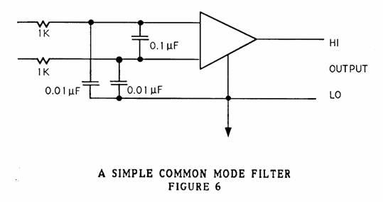
The simplest type of protection can be used when the required signal bandwidth is only to a few hertz. A very simple R-C filter inserted ahead of the amplifier will afford both common-mode- and normal-mode protection. Such a circuit for an amplifier having low input current is shown in Figure 6. It has a much lower normal-mode corner frequency than common-mode corner frequency. If this were not the case, the two common-mode R-C filter elements would have to be exactly matched to avoid converting common mode to normal mode at the frequencies where the mismatch in amplitude attenuation relative to frequency occurs. With the circuit shown, the normal-mode frequencies are greatly attenuated at this mismatched corner frequency.
If the required signal bandwidth extends to the kilohertz region, or more importantly, to frequencies near or beyond the amplifier’s common-mode slewing capability, the solution becomes much more difficult and less straightforward. If the amplifier is operated at higher gains, the relatively high amplitude of high-frequency common-mode signals requires a large attenuation of them so that they are not converted to a normal-mode signal offset by slew limiting in the input stage. This requires a filter which will reject high-frequency common-mode signals, yet will not affect the normal mode signals. It must also not convert the common-mode to a normal-mode signal.
The Solution
Such a passive filter, shown in Figure 7, was devised by Bill Gunning of Astrodata many years ago as an adaptation of the phantom circuit long used in long distance telephone circuits1. The filter unit, sometimes called a trifilar inductor, is constructed in such a way that the mutual coupling of the three windings is as near unity as possible. Thus any voltage of any frequency developed across one winding is exactly replicated in the other two. Therefore, any voltage on the third winding appears equally at each amplifier input terminal. If this voltage is the sensor common-mode voltage on the sensor end and the amplifier common-mode voltage on the amplifier end, then the two signal lines will also have the amplifier common-mode voltage on them or relative to the amplifier circuit, zero common-mode voltage.
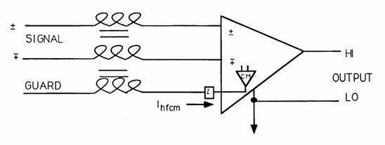
Figure 7
Expanding on the preceding description, in most amplifier designs, the low-frequency common-mode value is computed from the normal mode input signals. This voltage is then the common-mode voltage as recognized by the amplifier. This voltage is used by the amplifier to drive the input stage power supply at common mode, enhancing its low-frequency common-mode performance. Because of the relatively high power required to drive the input stage power supply, the common-mode amplifier’s slewing capability is usually limited to frequencies in the tens of kilohertz. It is bandwidth limited so that its slewing capability is not exceeded by the common-mode voltage. The amplifier’s common mode immunity is extended beyond these frequencies by the addition of the trifilar inductor (transformer).
The guard or shield lead has, by definition, the sensor-lead common-mode signal. The third winding of the transformer is connected between the sensor-lead guard and the amplifier’s common-mode point, thus causing any high-frequency voltage difference between the common-mode of the sensor and the amplifier common-mode to appear across the third winding of the transformer. A capacitor is placed in series with this winding so that little current flows through the transformer at low frequencies, avoiding core saturation. At high frequencies, the common mode signal is essentially zero at the amplifier’s input guard terminal because of the common mode amplifier’s bandwidth limiting. Because of the trifilar transformer, this common mode signal will be also essentially zero and equal at each differential input terminal. Thus the amplifier is not exposed to significant amounts high frequency common mode voltage.
As one might conclude, the explanation of the theory and the implementation of the concept are not equally simple. A properly designed filter circuit will become effective at frequencies at which the amplifier’s common mode capabilities begin to wane. The transformer must also have very low distributed capacitance so that the very high frequencies are not conducted across the filter to the amplifier input. Oft-times, a second smaller, lower inductance unit is required to extend the high-frequency performance.
So far, only data amplifiers have been identified as problem devices. The device doesn’t have to be an “amplifier” to have the described problem. Have you ever hooked two different model digital voltmeters sequentially to the same thermocouple or strain gage and observed two different readings? Or even connected two together to the same source and have two different readings? If so, you have again experienced errors caused by high-frequency common-mode. An oscilloscope, digital voltmeter or any other device intended to make low level measurements is likely to be susceptible. The fact that short leads are usually used with these devices is the saving factor in many applications.
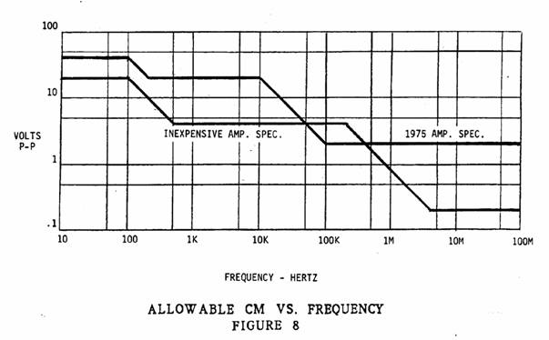
This discussion has included few quantitative numbers because there are so many factors which, when added together, result in error generation. A good philosophy for a well-managed test laboratory is to specify and purchase instrumentation equipment that will operate without significant error generation in the worst test conditions. As a result, the most unwary and inexperienced test engineer will not experience problems in acquiring meaningful test data. It is extremely difficult to identify when one has the best conditions, those that will result in no error generation in common-mode sensitive equipment. Past experience has shown that contaminated and questionable data are only discovered after the test setup has been torn down. Two common-mode immunity specifications are shown in Figure 8. The less stringent specification applies to a single card, common powered, computer controlled amplifier unit. The maximum offset allowed by either specification under the limits shown is 0.04% full scale.
Sensors Too?
Even less recognized is the fact that sensors, to a greatly varying degree, are also vulnerable to common-mode contamination. As luck would have it, the most susceptible designs are those that tend to be most used in the highest accuracy devices. These designs are those which contain active circuits to enhance their sensitivity to inductance, capacity or charge change, whichever is the device’s parameter of interest. These sensors include those used to measure pressure, acceleration and fluid flow, for example. Any change in the voltage between the circuit and the device case will be recognized by the circuit as a change in this monitored parameter and appear at the output as signal. Most of these devices contain an oscillator and they are extremely susceptible to common mode frequencies near the oscillator frequency or some multiple of it.
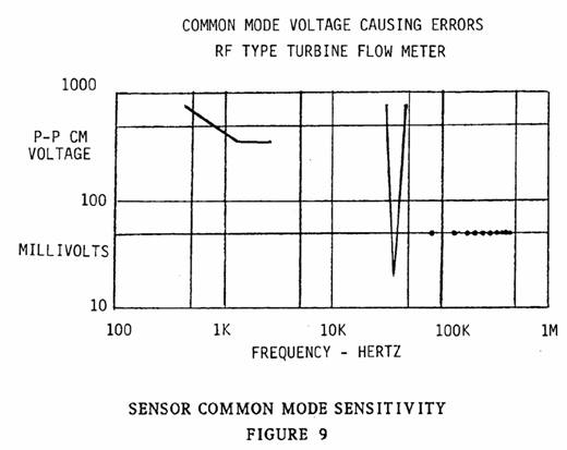
Figure 9 shows the sensitivity of a flow meter which contains an oscillator. As circuit guarding is unknown in such devices, the only readily apparent solution is to directly connect the circuit common and the sensor case. Since the signal source is now well grounded, the receiving device must accept the resulting common mode voltage. Many times the signal contains an undesirable amount of the sensor’s internal oscillator frequency as both common and normal mode voltage. Another application for the high-frequency common-mode-tolerant amplifier!
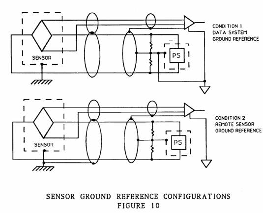
A recent experience demonstrated that even signals from common strain gage pressure sensors are sometimes contaminated by common-mode voltages. The subject sensor was being used to measure hydraulic pressure and significant error causing signals were observed which were related to the pump controller. Since strain gage sensors have floating bridges, the bridge supply was connected to the data system ground to control the dc common mode voltage seen by the amplifier. After moving the bridge supply reference to the transducer case, significantly less interference from the pump controller was experienced. These observations were made with an oscilloscope and no finite values were recorded. The difference in error observed was about an order of magnitude. Figure 10 shows these two ground configurations. This test demonstrated that also with a strain gage sensor, the sensor circuit must be referenced to the sensor case to minimize common mode induced errors. A high-frequency common-mode-resistant amplifier is a necessary component to complete the data system.
In summary, it might be stated that most testing situations contain significant amounts of high-frequency common-mode signals. In many cases, the desired data are contaminated because most common instrumentation is susceptible to high frequency common mode voltages (signals). You don’t even have to be in the aerospace business to qualify. Instrumentation is never far from computers or other RF trash generators. To find whether or not your data are so contaminated, you must look for it with some simple tests and perhaps as a result, buy some new, HFCM-resistant instruments.
Bibliography
Morrison, R., Grounding and Shielding Techniques in Instrumentation, Wiley, 1977
Morrison. R. & Lewis, W. H., Grounding and Shielding in Facilities. Wiley, 1990
Ott, H.W., Noise Reduction Techniques in Electronic Systems, Wiley, 1988. Note: This publication contains many excellent references.
1Tucker, D., A Technical History of Phantom Circuits. Proceedings of the IEE (UK), Vol. 126, No. 9, September 1979