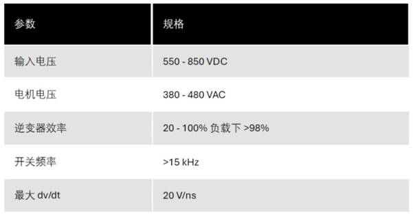
文章转自ADI官网,版权归属原作者一切
The best thing about being an applications engineer is the wide variety of customers, applications, circuits, and questions that I encounter, all of which provide me with daily opportunities to learn something new. Each year I receive several questions regarding the kind of performance users might expect from our amplifiers when their power supply is off. I like to refer to these amplifiers as “off-amps.”
Except for electrostatic discharge (ESD) testing, amplifiers are always characterized with the power on, so resolving off-amp problems isn’t always cut and dried. Answering off-amp questions requires a detailed understanding of the internal transistor-level workings of the amplifier, how the off-amp behaves without power, what external circuitry is connected to the off-amp, and how this peripheral circuitry behaves without power.
Strangely enough, most of the off-amp questions I receive do involve a voltage—but not the supply voltage. The voltage of interest is usually a voltage applied to either an input or output of the off-amp. To save power, users will selectively shut down certain parts of their systems. This often results in voltages being applied to un-powered parts of the system. Users are typically interested in knowing how the off-amp will react to this errant voltage, and what precautions they must take to ensure the safety of the off-amp.
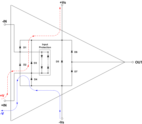
To understand how to protect an off-amp, we must first look at the ESD protection diodes, which are the amplifier’s first lines of defense. The ESD diodes protect the amplifier from short durations of high voltage, but can be damaged or destroyed by prolonged exposure to low dc voltages if the current through them is not limited. Figure 1 shows a typical op amp with ESD protection diodes.
Diodes D1 through D7 comprise the amplifier’s ESD protection network. The diodes shown inside the dashed line between ±IN form another protection network that protects the amplifier input stage from overvoltage conditions1. The number of series diodes in the anti-parallel network varies from amplifier to amplifier. To estimate the number of diodes between the inputs of an amplifier, look under Differential Input Voltage in the Absolute Maximum Ratings table in the amplifier datasheet.
When the amplifier power supplies are off, a voltage on ±IN can turn on diodes D1 through D4. Figure 1 shows the current paths from +IN through the protection diodes to the supplies, assuming the existence of a return path to ground. The red trace shows the path for a positive voltage to +Vs; the blue trace shows the path for a negative voltage to –Vs. Similar paths can be drawn from the output to the supplies through diodes D6 and D7, in cases where a voltage is present at the output of the off-amp. The most important safety precaution is to limit the current entering the off-amp’s pins.
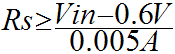
Without current limiting, the diodes and amplifier can be damaged or destroyed. We typically recommend limiting the current entering any amplifier pin to 5 mA or less. Often, all that must be added is a series resistor. Figure 2 shows the schematic for a current limited off-amp. Rs has little effect on the overall circuit function under normal operating conditions. Assuming the worse case scenario with ±Vs pins grounded, calculate Rs as shown in the following equation:
In another recent off-amp inquiry involving a FET-input amplifier, a user wanted to know whether an off-amp configured for unity gain would still present a high input impedance to a dc voltage at the noninverting input.
Like a diplomat, I answered, “Yes and no.” The off-amp input presents a high input impedance for voltages less than 0.6 V because the ESD diodes need at least 0.6 V to conduct. Without a conduction path, the input still appears as a high impedance. If the input voltage were greater than 0.6 V, however, current would start to flow through the ESD diodes and other “sneak paths” within the off-amp. To limit the current flow in D3, use the equation to solve for Rs. With a worse case of 4 V applied to the off-amp input, Rs must be at least 680 ohms, not exactly a high input impedance.
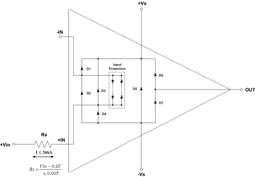
Reverse polarity protection can help in these applications. As a former designer of defense electronics, reverse polarity protection was something that I routinely incorporated into my designs. Reverse polarity protection ensures that the circuit is safe even when the wrong polarity supplies are connected to the bias pins of the system. Incorporating reverse polarity protection is a simple, low-cost insurance policy; all it takes is a pair of diodes. If the correct power supply polarity is applied, the diodes are forward biased and the circuit works as expected. If the opposite power supply polarity is applied, the diodes are reverse biased. No current can pass and the circuit is protected. Figure 3 shows an amplifier with reverse polarity protection diodes.
Reverse polarity protection diodes also allow a high input impedance to be achieved over a larger input range because the diodes add an additional voltage drop that must be overcome before current can flow. Preventing current flow through D3 to the +Vs pin is elegantly accomplished by external diode RPD1. For positive voltages, RPD1 is reverse biased, therefore preventing current flow through D3. Current does not flow from the input to the negative rail through ESD diode D4, which is reverse biased, but it seeks another path through the PN junction of the FET input stage. Diode RPD2 forms an additional voltage barrier that must be overcome before any current can flow.
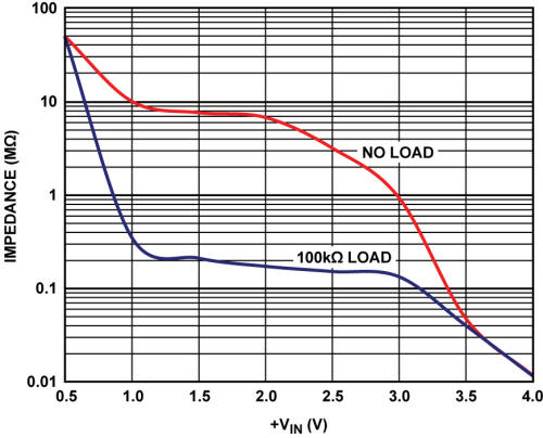
Figure 4 shows the test circuit used for measuring the input impedance of the off-amp. Note that Rs is larger than required by the equation. The larger resistor limits the current even more and, equally important, it was readily available in the lab.
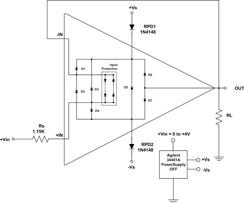
Figure 5 shows the input impedance of the FET off-amp without the reverse polarity protection diodes. The input impedance decreases as the increasing bias turns D3 on harder.
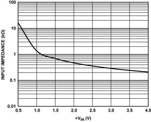
Figure 6 shows the input impedance for two different load conditions with the reverse polarity protection diodes in place. Note that the Y-axis in Figure 6 is in M ohms rather than K ohms, as used in Figure 5. The reverse polarity protection diodes provide three orders of magnitude improvement. The breakpoints indicate different junctions within the off-amp being turned on as the input voltage increases. The reverse polarity protection diodes help increase the thresholds for the break points. The value of the load impedance is an important consideration in this application. A low impedance shunt load to ground will provide a parallel low impedance path for current flow and render this approach useless. Thus, the user must understand how the off-amp behaves with no power, and how the adjacent circuitry behaves as well.
Getting to the bottom of off-amp questions can be challenging, with many factors that must be taken into account. The amplifier type, peripheral circuitry, and input and output voltages are all important. The best way to protect an off-amp is to ensure that the power to any circuit that touches the off-amp is off as well. If that’s not possible, then make sure to limit the current entering the off-amp. Always check with the applications engineer if you need additional help.
参阅电路
1Amplifier Input Protection… Friend or Foe? John Ardizzoni, Analog Dialogue 41-05, May, 2007