1 概述
本规划已实用于国家863方案“可扩展到T比特的高性能IPv4/v6路由器根底渠道及试验体系”项目中。其主要功用是对主控部分的FPGA读取Flash进行操控。
在本项目中,主控部分的FPGA在重启时需求从Flash中下载初始化程序。当下载完结后,FPGA仍会根据需求从Flash相应地址读取数据。这就要求在FPGA和Flash之间有一块操控逻辑来操控对Flash的读取。本规划便是完结的对这块操控逻辑的详细完成。
本文用VHDL言语在CPLD内部编程将其完成。本文第2节给出用VHDL言语在CPLD内部编程完成Flash读取的进程,第3节对全文进行归纳总结。
2 完成
2.1 器材的挑选
咱们选用Xilinx公司XC9500XL 3.3V ISP 系列XC95288XL-7TQ144I芯片。XC95288xl是一个3.3V的低电压、高效的CPLD,在通讯和计算机体系中的有广泛的运用。它包括16个54V18个功用块,供给了6400个可用的门电路,这些门电路的传达延时为6ns.
关于Flash,项目中挑选了Intel公司的Intel StrataFlash系列的256-Mbit J3型Flash.其数据宽度可别离支撑8位或许16位。
2.2 完成中的问题及处理办法
项目中选用的Flash的输出为16位,而向FPGA输出的数据为32位,因而产了数据宽度不匹配的问题,处理的办法有两种:
榜首 运用两块相同的Flash,别离将其输出的数据送入FPGA接口的高16位和低16位;其缺陷是需求添加一块Flash,然后本钱添加。
第二 选用下降读取速度的办法,把从一块Flash中接连两次读取的16位数据拼接起来,组成一组32位的数据后送入FPGA接口。
出于对本钱和复杂度的考虑,在此规划中咱们采取了第二种办法加以完成。
2.3 根本规划模块图
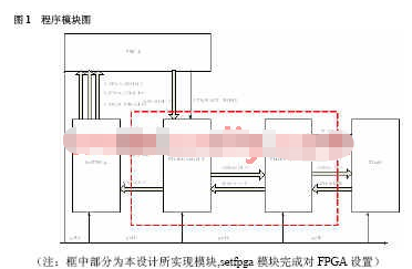
2.4 用VHDL进行完成(注:实体部分界说可别离拜见模块图中的区分)
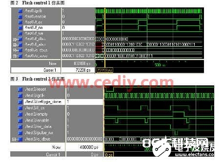
Flash control 1
process(reset,gclk)
begin
if reset =‘0’ then
count_reset 《=‘0’;
elsif gclk‘event and gclk =’1‘ then
count_reset 《= not(count(4) and count(3) and count(2));
end if;
end process;
process(count_reset,gclk)
begin
if count_reset =’0‘ then
count 《=(others =》’0‘);
elsif gclk’event and gclk =‘1’ then
count 《=count +1;
end if;
end process;
process(count_reset,reset,enable)
begin
if reset =‘0’ then
F_CS 《=‘1’;
F_OE 《=‘1’;
F_WE 《=‘1’;
elsif count_reset =‘0’ then
F_CS 《= ‘1’;
F_OE 《= ‘1’;
F_WE 《= ‘1’;
elsif enable‘event and enable =’1‘ then
F_Abus 《= C_Abus;
F_CS 《= ’0‘;
F_OE 《= ’0‘;
F_WE 《= ’1‘;
C_Dbus 《= F_Dbus;
end if;
end process;
Flash control 2
d_count_rst 《= not(d_count(1) and (not d_count(0)) and empty);
sig_WD 《= not(d_count(1) and (not d_count(0)));
WR_DATA 《= sig_WD;
process(gclk,d_count)
begin
if reset =’0‘ then
d_count 《= ’1‘;
elsif F_CS = ’1‘ then
d_count1 《= not d_count1 ;
if gclk’event and gclk =‘1’ then
d_count2 《= d_count1;
d_count 《= d_count2;
end if;
end if;
end process;
process(reset,d_count,C_Dbus)
begin
if reset = ‘0’ then
data_adder 《= (others =》‘0’);
elsif d_count‘event and d_count = ’0‘ then
data_adder(31 downto 16) 《= C_Dbus;
elsif d_count’event and d_count = ‘1’ then
data_adder(15 downto 0) 《= C_Dbus;
end if;
end process;
enable 《= enable1 and enable2;
process(reset,d_count,F_CS)
begin
if reset = ‘0’ or F_CS = ‘0’ then
enable1 《= ‘1’;
enable2 《= ‘1’;
elsif d_count‘event then
if gclk’event and gclk =‘1’ then
enable1 《= ‘0’;
enable2 《= not enable1;
end if;
end if;
end process;
process(reset,F_CS)
begin
if reset = ‘0’ then
address《= X“400000”;
elsif F_CS = ‘1’ then
C_Abus 《= address;
address 《= adderss +1;
end if;
end process;
process(reset,F_CS)
begin
if reset = ‘0’ then
address《= X“400000”;
data_adder 《=(others =》‘0’);
elsif F_CS = ‘1’;
address 《= adderss +1;
end if;
end process;
process(d_count2,F_CS)
begin
if F_CS = ‘0’ then
enable1 《= ‘1’;
enable 《= ‘1’;
elsif d_count2 = “00” or d_count2 = “01” then
enable 《= ‘0’;
end if;
end process;
process(gclk,sig_WD)
begin
if sig_WD = ‘1’ then
Pulse_RW 《=‘1’;
elsif gclk‘event and gclk =’1‘ then
W_D1 《= sig_WD;
W_D2 《= W_D1;
if empty =’0‘ then
data_adder1 《= data_adder;
Pulse_RW 《= (W_D1 or (not W_D2));
end if;
end if;
end process;
(注:此程序在Xilinx公司的ISE6.2i环境下用VHDL编程完成,其仿真波形见下图)
3 结束语
在实践运用中,以此CPLD对Flash的读取进行操控。仿真成果及最终的实践调试都标明该规划契合项目的要求。在程序中经过对读取的记数操控,本规划能够在不添加Flash片数的情况下支撑16/32/64位的数据输出宽度。能够节省必定的本钱,具有适当的灵活性和实用性。
责任编辑:gt