AD5379相关信息来自ADI官网,详细参数以官网发布为准,AD5379供给信息可在查IC网查找相关供给商。
产品概况
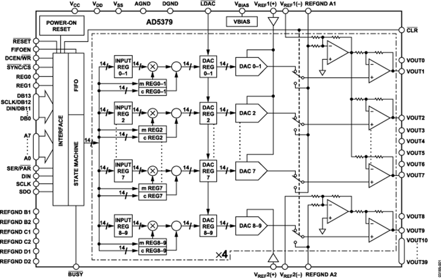
The AD5379 contains 40 14-bit DACs in one CSPBGA package. The AD5379 provides a bipolar output range determined by the voltages applied to the VREF(+) and VREF(−) inputs. The maximum output voltage span is 17.5 V, corresponding to a bipolar output range of −8.75 V to +8.75 V, and is achieved with reference voltages of VREF(−) = −3.5 V and VREF(+) = +5 V.
The AD5379 offers guaranteed operation over a wide VSS/VDD supply range from ±11.4 V to ±16.5 V. The output amplifier headroom requirement is 2.5 V operating with a load current of 1.5 mA, and 2 V operating with a load current of 0.5 mA.
The AD5379 contains a double-buffered parallel interface in which 14 data bits are loaded into one of the input registers under the control of the WR, CS, and DAC Channel Address Pins A0 to A7. It also has a 3-wire serial interface that is com-patible with SPI®, QSPI™, MICROWIRE™, and DSP® interface standards and can handle clock speeds of up to 50 MHz.
The DAC outputs are updated upon reception of new data into the DAC registers. All the outputs can be simultaneously updated by taking the LDAC input low. Each channel has a programmable gain and an offset adjust register.
Each DAC output is gained and buffered on-chip with respect to an external REFGND input. The DAC outputs can also be switched to REFGND via the CLR pin.
Applications
- Level setting in automatic test equipment (ATE)
- Variable optical attenuators (VOA)
- Optical switches
- Industrial control systems
优势和特色
|
|
AD5379电路图
AD5379中文PDF下载地址
AD5379下载链接地址:https://www.analog.com/media/en/technical-documentation/data-sheets/AD5379.pdf


